
Two-dimensional lead-free perovskite material and design method

A perovskite material, lead-free perovskite technology, applied in molecular design, computer materials science, instruments, etc., can solve the problems of only 6.2%, high mobility, and large environmental pollution, and achieve excellent transport characteristics, The effect of high light absorption coefficient and great commercial value

Inactive Publication Date: 2020-01-10
北京状元府影视文化传媒有限公司
View PDF5 Cites 8 Cited by
  • Summary
  • Abstract
  • Description
  • Claims
  • Application Information

AI Technical Summary

Problems solved by technology

At present, the most mainstream light-absorbing layer material of perovskite solar cells is methylamine lead iodide (MAPbI 3 ) as the representative lead-based hybrid perovskite, although its properties are good, there are still two problems to be solved on the road to industrialization: 1. The current perovskite materials have poor stability and are exposed to Light, heat, or water and oxygen environments can easily lead to unstable device performance; 2. Lead-based perovskite materials contain highly toxic element lead, which pollutes the environment and can cause irreversible damage to the human nervous system
The successful preparation of graphene has opened the door to the two-dimensional world. As an ideal material for nano-optoelectronic devices, graphene has ultra-high carrier mobility (10 4 -10 5 cm 2 V -1 the s -1 ), but its zero bandgap greatly limits its application in the semiconductor industry
At present, people mainly solve this problem in two ways: first, open the bandgap value of graphene through a series of external conditions such as doping, strain, electric field, and construction of heterojunction; Difficulty maintaining graphene's linear electron dispersion and ultrahigh mobility while opening the bandgap
At present, the external quantum efficiencies of green, red, and near-infrared LEDs are 20.3%, 21.3%, and 20.7%, respectively, while the external quantum efficiency of blue LEDs is only 6.2%.

Method used


Image

  • Two-dimensional lead-free perovskite material and design method
  • Two-dimensional lead-free perovskite material and design method
  • Two-dimensional lead-free perovskite material and design method

Examples


Embodiment Construction

[0068] In order to make the purpose, technical solutions and advantages of the embodiments of the present invention clearer, the technical solutions in the embodiments of the present invention will be clearly and completely described below in conjunction with the drawings in the embodiments of the present invention. Obviously, the described embodiments It is a part of embodiments of the present invention, but not all embodiments. Based on the embodiments of the present invention, all other embodiments obtained by persons of ordinary skill in the art without making creative efforts belong to the protection scope of the present invention.

[0069] Below in conjunction with accompanying drawing, the present invention is described in further detail:

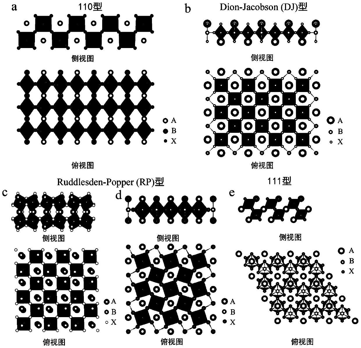
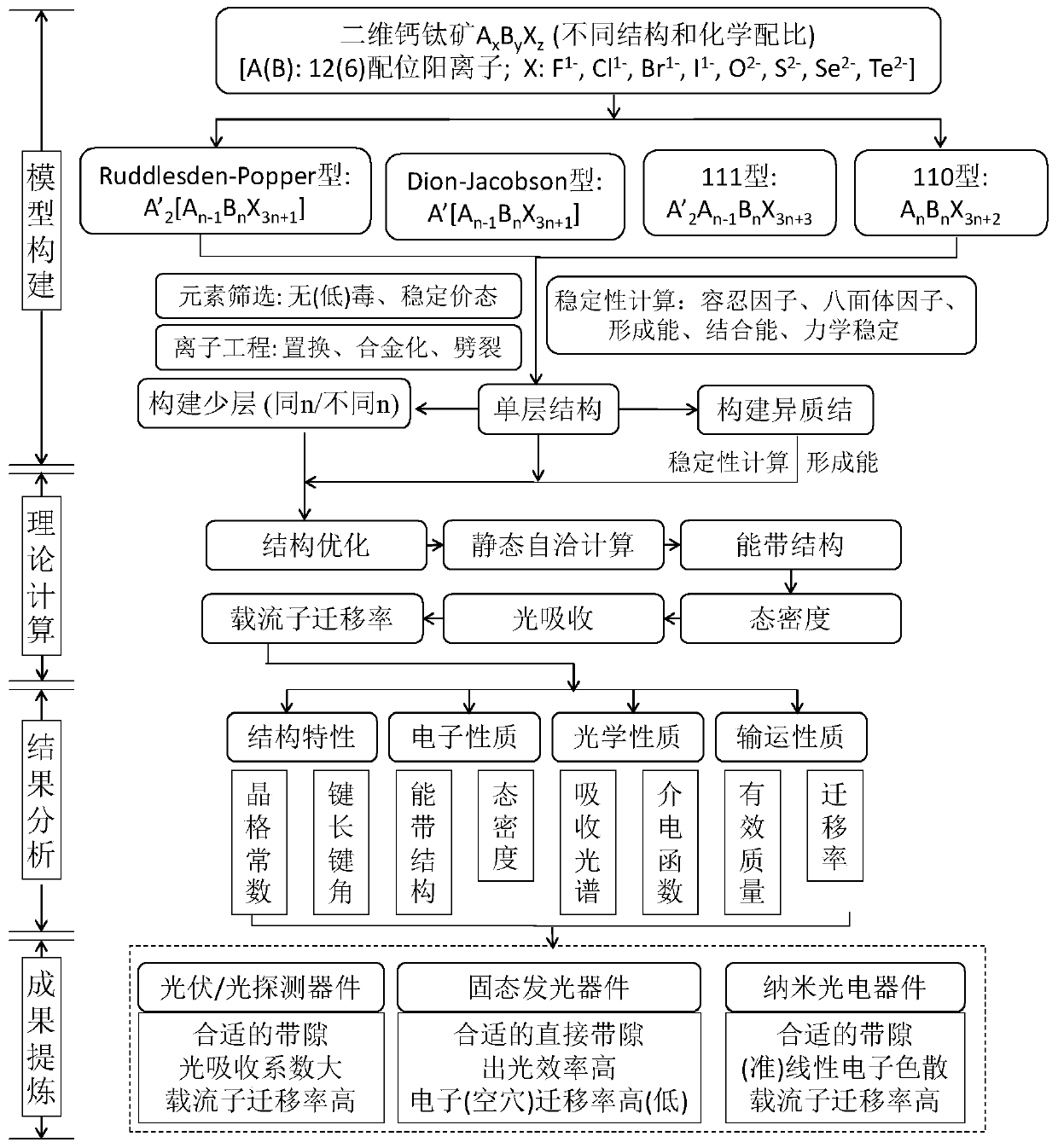
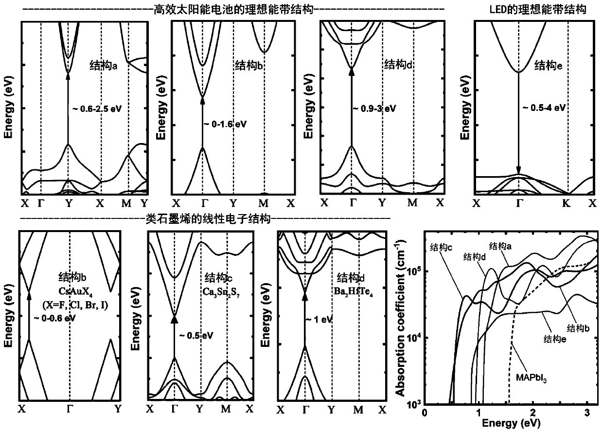
[0070] The invention provides a two-dimensional lead-free perovskite material and a design method. The designed two-dimensional lead-free perovskite material includes lead-free perovskite-type halide and chalcogenide semiconductor ma...


PUM

PropertyMeasurementUnit
band gapaaaaaaaaaa
external quantum efficiencyaaaaaaaaaa

Abstract

The invention discloses a two-dimensional lead-free perovskite material and a design method. The structural formula of the two-dimensional lead-free perovskite material is expressed as: AxByXz, wherein x = 1, 2, 3; y = 1, 2 ; Z = 4, 7, 8, 9; A is one element of Cs, Ba, Sr, and Ca; B is one element of Sb, Bi, Ga, In, Au, Sn, Hf, Zr, amd Ti; X is one element of F, Cl, Bre, I, S, Se, and Te. A firstprinciple method that is widely used, accurate in computation, and low in cost is used to systematically compute the excellent properties of such structure, and two types of perovskite materials, including transcending solar photovoltaic star material MAPbI3 and a graphene-like semiconductor with graphene linear electronic dispersion and an intrinsic quasi-particle bandgap of about 0.1 to 1 eV, are found out.

Description

technical field [0001] The invention relates to the technical fields of energy and semiconductor materials, in particular to a two-dimensional lead-free perovskite material and a design method. Background technique [0002] With the continuous development of science and technology and the continuous progress of society, energy problems have become increasingly prominent, and the development of the semiconductor industry has also reached a certain bottleneck period. Perovskite materials, as a hot material that has received more and more attention in recent years, have shown many excellent properties, and have played a vital role in both energy issues and the development of the semiconductor industry. [0003] First of all, regarding energy issues, since solar energy is an inexhaustible clean energy source, it is an important countermeasure for us to pursue sustainable development. Solar cells are a way to directly convert solar energy into electrical energy, and have attract...

Claims


Application Information

Patent Timeline
Patent Type & Authority Applications(China)
IPC IPC(8): G16C60/00G16C20/50
CPCG16C60/00G16C20/50
Inventor 刘海云
Owner 北京状元府影视文化传媒有限公司
Learn More