

TFT substrate and its preparation method, display device
A substrate and substrate substrate technology, applied in semiconductor/solid-state device manufacturing, semiconductor devices, electrical components, etc., can solve problems such as unevenness, side etching, and fast etching of copper film layers, so as to prevent damage and prevent side Eclipse effect
- Summary
- Abstract
- Description
- Claims
- Application Information
AI Technical Summary
Problems solved by technology
Method used
Image

Examples
preparation example Construction
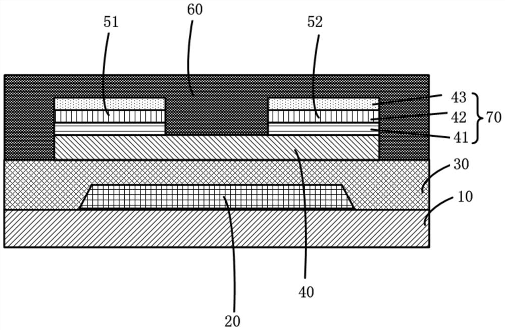
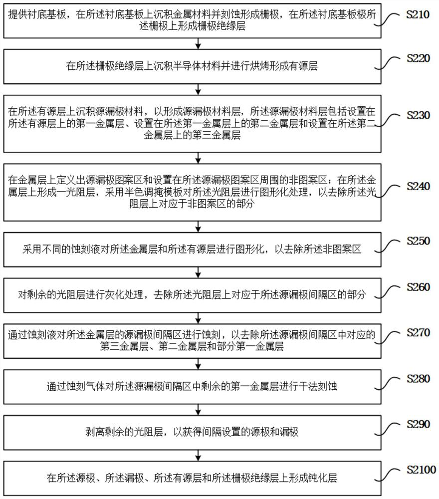
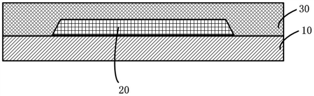
[0040] In addition, the present invention provides a method for preparing a TFT substrate, comprising the steps of: depositing a metal material on a base substrate; patterning the metal material to form a gate; forming a gate insulation on the base substrate layer to cover the patterned gate; an active layer is formed on the gate insulating layer and located above the gate; a first metal layer, a first metal layer, a A second metal layer and a third metal layer, wherein the first metal layer is made of metal material, the second metal layer is made of nickel or nickel alloy, and the third metal layer is made of copper material ; and patterning the first metal layer, the second metal layer, the third metal layer and the active layer by applying glue, exposing and etching to form patterned source electrodes, drain electrodes and active layers.
[0041] Further, after the step of forming the patterned source electrode, drain electrode and active layer, the method further includes...
PUM
| Property | Measurement | Unit |
|---|---|---|
| thickness | aaaaa | aaaaa |
Abstract
Description
Claims
Application Information