

GaN-based photothermal detection thin film element
A thin-film element and photothermal detection technology, which is applied in the direction of electric radiation detectors, can solve the problems of high-power continuous photothermal detection requiring refrigeration, thermal radiation detection wavelength range is narrow, and it is difficult to mass-produce, achieving good linearity, The effect of wide wavelength range and fast response speed
- Summary
- Abstract
- Description
- Claims
- Application Information
AI Technical Summary
Problems solved by technology
Method used
Image

Examples
Embodiment 1
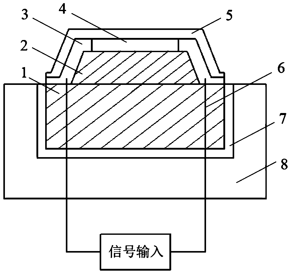
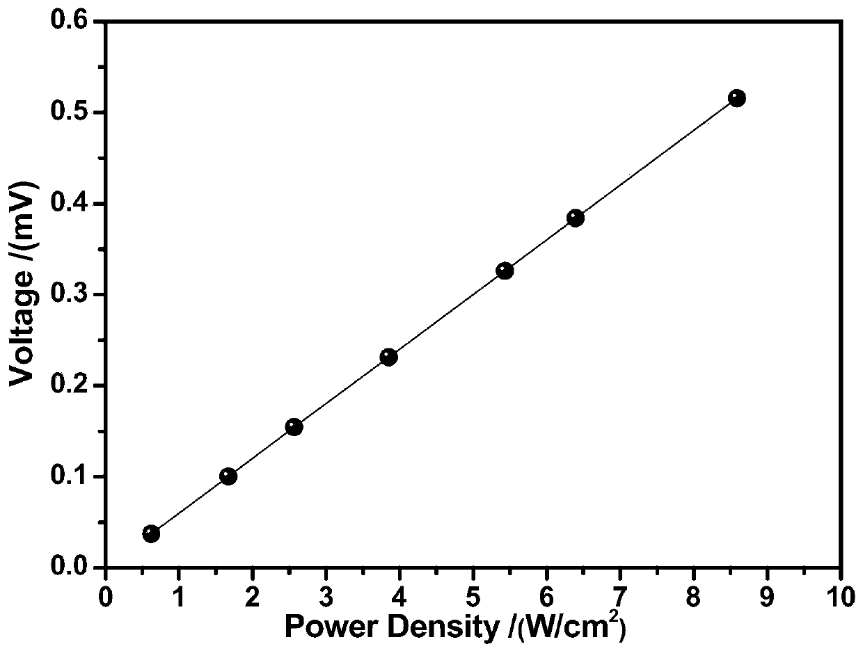
[0026] A GaN-based photothermal detection thin film element, used for 0.8-12μm continuous infrared thermal radiation detection, with a structure such as figure 1 As shown, the thin film element structure includes: single crystal substrate 1, [p-GaN / n-GaN] N Superlattice 2 , metal electrode 3 , absorbing layer 4 , anti-reflection protection layer 5 , lead wire 6 , thermal conductive adhesive 7 , and heat sink 8 . The single crystal substrate is a 5° beveled semi-insulating GaN (0001) substrate with a room temperature resistivity of 1.0E+7Ω·cm and a thickness of 0.2mm. [p-GaN / n-GaN] N The superlattice is alternately epitaxially grown on a 5° off-cut semi-insulating GaN (0001) substrate by MOCVD, cut off by the p-GaN plane and etched trapezoidal mesas, along the [p-GaN / n-GaN] NA pair of Au electrodes are set on both sides of the superlattice and GaN (0001) substrate in the c-axis tilt direction to form ohmic contacts, which are derived from the Au leads and connected to the sig...
Embodiment 2
[0030] A GaN-based photothermal detection thin-film element, used for 0.35-0.8μm continuous light-ray detection, the structure of the thin-film element includes: single crystal substrate, [p-GaN / n-GaN] N Superlattices, metal electrodes, absorber layers, anti-reflective protective layers, leads, thermal paste, and heat sinks. The single crystal substrate is a 20° chamfered semi-insulating SiC (0001) substrate with a room temperature resistivity of 2.0E+7Ω·cm and a thickness of 0.4mm. [p-GaN / n-GaN] N The superlattice is alternately epitaxially grown on a 20° off-cut semi-insulating SiC (0001) substrate by MOCVD, cut off by the p-GaN plane and etched trapezoidal mesa, along the [p-GaN / n-GaN] N A pair of Ti / Al / Pt / Au combined electrodes are arranged on both sides of the superlattice and SiC (0001) substrate in the c-axis tilt direction to form an ohmic contact, which is derived from the Cu lead and connected to the signal input end, and the absorption layer is covered in [ p-GaN / ...
Embodiment 3
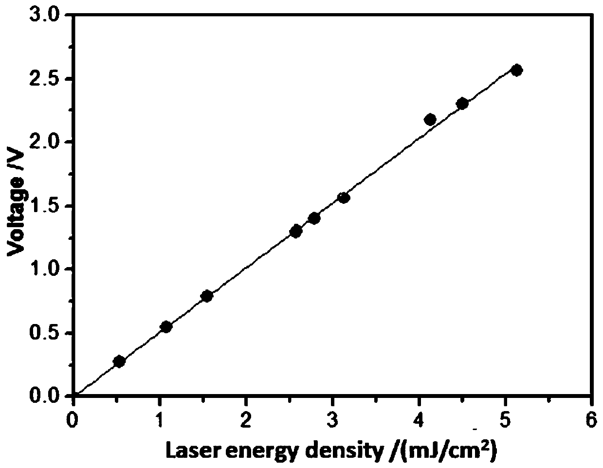
[0034] A GaN-based photothermal detection thin film element for 365nm monochromatic pulsed laser detection, the structure of the thin film element includes: single crystal substrate, [p-GaN / n-GaN] N Superlattice, metal electrodes, absorber layer, anti-reflection protective layer, leads, thermal paste, heat sink. Single crystal substrate is 45° bevel cut insulating Al 2 o 3 (0001) substrate, the resistivity at room temperature is 1.0E+8Ω·cm, and the thickness is 0.8mm. [p-GaN / n-GaN] N Alternative epitaxial growth of superlattice on 45° off-cut insulating Al by MOCVD 2 o 3 On the (0001) substrate, cut off the p-GaN surface and etch the trapezoidal mesa, along the [p-GaN / n-GaN] N Superlattice and Al 2 o 3 (0001) A pair of Ag electrodes are arranged on both sides of the c-axis inclined direction of the substrate to form an ohmic contact, which is derived from the Ag lead and connected to the signal input end. Since the element is used for deep ultraviolet monochromatic ligh...
PUM
| Property | Measurement | Unit |
|---|---|---|
| Thickness | aaaaa | aaaaa |
| Thickness | aaaaa | aaaaa |
| Diameter | aaaaa | aaaaa |
Abstract
Description
Claims
Application Information