A nanocrystalline silicon oxide film and a photoresist-like silicon oxide material prepared therefrom

A technology of crystalline silicon oxide and colloidal silicon oxide, which is applied in the field of microelectronics and solar cells, can solve problems such as pollution in the deposition process, achieve the effects of simplifying the preparation process, reducing the deposition temperature, and overcoming the incompatible defects exposed

Active Publication Date: 2021-11-23
NINGBO UNIV
View PDF6 Cites 0 Cited by
  • Summary
  • Abstract
  • Description
  • Claims
  • Application Information

AI Technical Summary

Problems solved by technology

Plasma chemical vapor deposition is a common method for forming thin films on substrates, but the introduction of photoresist in PECVD pollutes its deposition process
[0005] In summary, the existing photolithography technology has certain limitations

Method used


Image

  • A nanocrystalline silicon oxide film and a photoresist-like silicon oxide material prepared therefrom
  • A nanocrystalline silicon oxide film and a photoresist-like silicon oxide material prepared therefrom
  • A nanocrystalline silicon oxide film and a photoresist-like silicon oxide material prepared therefrom

Examples


Embodiment 1

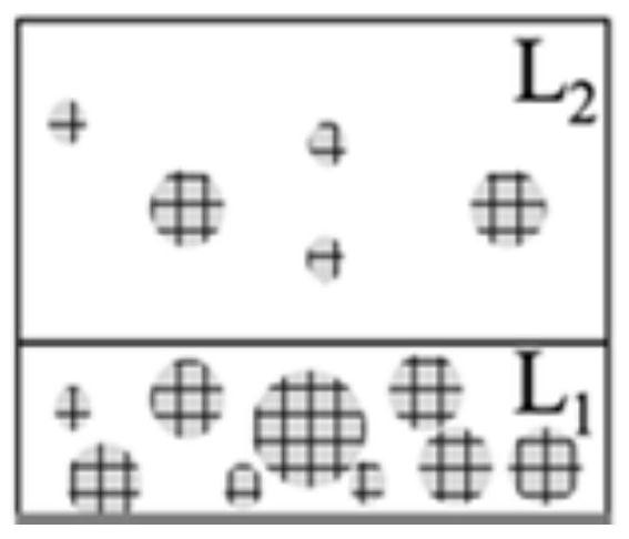
[0048] like figure 1 As shown, a nanocrystalline silicon oxide film, the nanocrystalline silicon oxide film is a multi-layer film formed by embedding silicon nanocrystals in a hydrogenated amorphous silicon oxide matrix, and the multi-layer film sequentially includes L1 layer and For the L2 layer, the refractive index of the L1 layer is 2.3 at 600 nm, and the refractive index of the L2 layer is 1.6 at 600 nm; the thickness of the L1 layer is 50 nm, and the thickness of the L2 layer is 90 nm; among them, the volume fraction of silicon nanocrystals in the L1 layer larger than the volume fraction of silicon nanocrystals in the L2 layer.

Embodiment 2

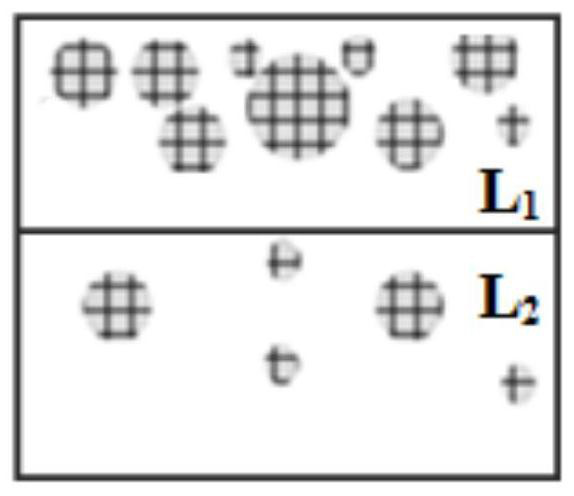
[0050] like figure 2 As shown, a nanocrystalline silicon oxide film, the nanocrystalline silicon oxide film is a multi-layer film formed by embedding silicon nanocrystals in a hydrogenated amorphous silicon oxide matrix, and the multi-layer film sequentially includes L2 layer and L1 layer, the refractive index of L1 layer is 2.9 at 600 nm, and the refractive index of L2 layer is 1.8 at 600 nm; the thickness of L1 layer is 60 nm, and the thickness of L2 layer is 80 nm; among them, the volume fraction of silicon nanocrystals in L1 layer is larger than the volume fraction of silicon nanocrystals in the L2 layer.

Embodiment 3

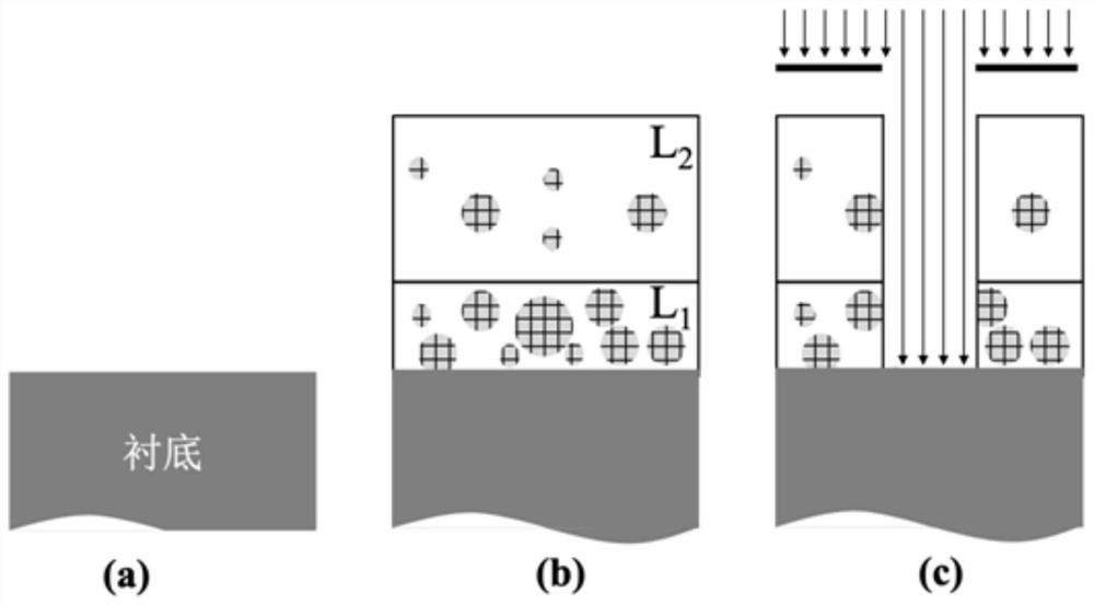
[0052] like image 3 As shown, a photoresist-like silicon oxide, the preparation method of which comprises the following steps:

[0053] Prepare glass substrates (Corning 1737) as image 3 (a);

[0054] First deposit the L1 layer on the substrate, deposition temperature: 150°C, pressure: 2.0 Torr, power density: 100mW / cm 2 , SiH 4 : 12SCCM, H 2 : 200SCCM, CO 2 : 5SCCM, thickness is 50nm; then deposit L2 layer on L1 layer, temperature: 150℃, pressure: 2.0Torr, power density: 100mW / cm 2 , SiH 4 : 12SCCM, H 2 : 200SCCM, CO 2 : 15SCCM with a thickness of 90nm; such as image 3 (b), wherein the refractive index n1 of the L1 layer is 2.3 (600 nm), and the refractive index n2 of the L2 layer is 1.6 (600 nm);

[0055] Ultraviolet laser ablation: Align the mask according to the desired pattern, and then perform laser exposure to obtain a photoresist-like silicon oxide material, such as image 3 (c).

[0056] The absorbance of the above nanocrystalline silicon oxide bilayer...


PUM

PropertyMeasurementUnit
thicknessaaaaaaaaaa
thicknessaaaaaaaaaa
refractive indexaaaaaaaaaa

Abstract

The invention belongs to the technical field of microelectronics and solar cells, and relates to a photoresist-like silicon oxide material and a preparation method thereof. The photoresist-like silicon oxide material includes a substrate and a nanocrystalline silicon oxide film nc-SiO x , the nanocrystalline silicon oxide film is a double-layer structure, including the first film with high solubility and low absorption rate and the second film with high absorption rate and low solubility, wherein the refractive index n1 of the first film is greater than that of the second film The refractive index of the film. The preparation method of the photoresist-like silicon oxide material includes preparing the substrate, depositing a silicon oxide double-layer film, ultraviolet laser ablation, removing nc-SiO x . The double-layer nanocrystalline silicon oxide film of the present invention increases the absorptivity of the photoresist film without reducing the solubility. At the same time, the film is coated by radio frequency plasma extraction enhanced chemical vapor deposition, which overcomes the problem of photoresist Defects that are incompatible with high temperature and plasma exposure greatly simplify the fabrication process.

Description

technical field [0001] The invention belongs to the technical field of microelectronics and solar cells, and relates to a new dielectric structure and a preparation process thereof, in particular to a nanocrystalline silicon oxide film and a photoresist-like silicon oxide material prepared therefrom. Background technique [0002] Photolithography technology refers to the photoresist (photoresist) as an intermediate medium under the action of light, through exposure, development, etching and other processes, and finally transfers the image information designed on the mask to the wafer. Or a process on the dielectric layer. Photolithography is an important process in the production of planar transistors and integrated circuits. Patterning can be well controlled by exposure. It has been widely used in the crystalline silicon industry, such as microelectronics and solar cells, and other fields based on semiconductor materials. [0003] Photoresist is a photosensitive material i...

Claims


Application Information

Patent Timeline
Patent Type & Authority Patents(China)
IPC IPC(8): C23C16/50C23C16/40C23C16/56C23C16/52H01L21/027
CPCC23C16/402C23C16/50C23C16/52C23C16/56H01L21/027
Inventor 陈王华郑珍张晓伟
Owner NINGBO UNIV
Why Eureka
Try Eureka