Electromagnetic shielding coating method

An electromagnetic wave and metal technology, applied in the direction of magnetic/electric field shielding, coating, electrical components, etc., can solve the problems of inability to separate the coating layer, cannot be formed normally, low reuse rate, etc., and achieve excellent electromagnetic wave shielding performance, tightness Excellent adhesion and low cost effect

Active Publication Date: 2020-02-14
维洲TNC株式会社
View PDF9 Cites 0 Cited by
  • Summary
  • Abstract
  • Description
  • Claims
  • Application Information

AI Technical Summary

Problems solved by technology

[0010] However, for the above-mentioned technology, since it is necessary to form a multilayer metal layer, there is a problem that the process is complicated. For a plated film and a coating layer formed by laminating a multilayer metal layer, if one of the multiple layers If the side layer is partially unqualified or fails to form a uniform coating, the layer stacked above it will not be formed normally in the subsequent steps
In particular, a plurality of layers are each composed of a metal layer, so in the case of a defect, the coating layer cannot be separated from the material to be coated, and the cost loss in the process is very high due to the high defect rate and low recycling rate. big problem

Method used


Image

  • Electromagnetic shielding coating method
  • Electromagnetic shielding coating method
  • Electromagnetic shielding coating method

Examples


Embodiment 1

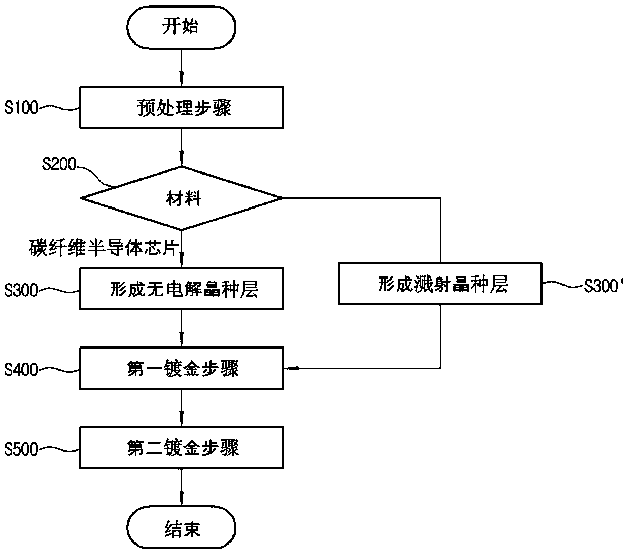
[0078] At a temperature of about 180°C, maintain 10 -5 mmHg to 10 -3 The surface of the semiconductor chip is irradiated with surface plasma with 99% oxygen at a vacuum degree of mmHg, and after that, carbon tetrafluoride (CF 4 ) gas etches the surface of the material.

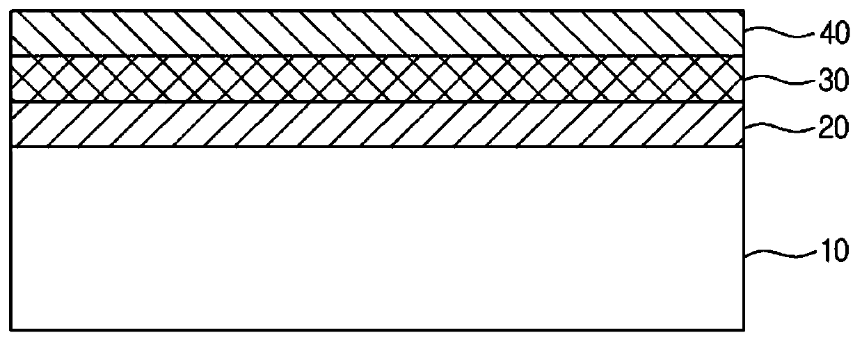
[0079] Put the surface of the semiconductor chip through the above steps into an aqueous solution of palladium sulfate at a temperature of 55° C. and a concentration of 7 g / L. After adding an aqueous solution of sodium hypophosphite so that the concentration becomes 3 g / L, immerse it for 8 minutes. A seed layer is formed.

[0080] Take out the semiconductor chip and place it in an aqueous copper chloride solution with a temperature of 30°C and a concentration of 80g / L, add sodium hypophosphite solution, and immerse it for 5 minutes. The ammonium acid hydrate aqueous solution was immersed for 30 minutes to form an electromagnetic wave shielding coating layer.

Embodiment 2

[0082] Except in the 10×10cm woven carbon fiber 2 An electromagnetic wave shielding coating layer was formed in the same manner as in Example 1 except that the surface of the carbon fiber fabric was subjected to the electromagnetic wave shielding coating method of the present invention instead of the semiconductor chip. A semiconductor package was prepared by allowing the carbon fiber fabric formed with the coating layer to completely surround the semiconductor surface.

Embodiment 3

[0084] At a temperature of about 180°C, maintain 10 -5 mmHg to 10 -3 Surface plasma irradiation is performed on the surface of the semiconductor chip for smart cars with 99% oxygen at a vacuum degree of mmHg.

[0085] On the surface of the plasma-treated material, with nickel and iron as target substances, at a temperature of 195°C and 10 - 5 mmHg to 10 -3 Under the condition of vacuum degree of mmHg, the plasma sputtering process was performed on nickel and iron as the target substances at a power of 1.5 kW. Put the above-mentioned semiconductor chip for smart cars into an aqueous copper chloride solution with a temperature of 30°C and a concentration of 80g / L, and add a sodium hypophosphite solution and then immerse it for 5 minutes. Then, at a temperature of 75°C and a concentration of A 40 g / L ammonium tungstate hydrate aqueous solution was immersed for 30 minutes to form an electromagnetic wave shielding coating layer.


PUM

PropertyMeasurementUnit
thicknessaaaaaaaaaa
thicknessaaaaaaaaaa
thicknessaaaaaaaaaa

Abstract

Provided is a method for performing an electromagnetic interference shielding coating operation on the surface of a metal or a nonmetal material, comprising: a pre-process step of cleaning the surfaceof the material and performing a dry surface etching operation before coating; a surface seed replacement forming step of forming a metal seed layer on the pre-processed surface; a first plating stepof performing an electroless plating operation on a surface of the seed layer by a first metal having a basic shielding function; and a second plating step of performing an electroless plating operation on a surface of the first metal plating layer by a second metal having a finishing shielding function, wherein the first metal is copper (Cu) and the second metal is tungsten (W). The present invention provides the electromagnetic interference shielding coating method which can be applied to the surface of components of a smart car, a mobile device and a wearable device, and has excellence inan electromagnetic interference shielding effect, coating durability, manufacturing time and economic feasibility for costs.

Description

technical field [0001] The present invention relates to an electromagnetic wave shielding coating method. As a method for performing electromagnetic wave shielding coating on the surface of metal or non-metallic materials, the present invention is characterized in that it includes: a pretreatment step of cleaning the material surface, before coating , performing dry surface etching; surface seed crystal replacement molding step, forming a metal seed layer on the pretreated surface; the first gold plating step, using the first metal to perform electroless gold plating on the surface of the seed layer to achieve basic shielding Function; and the second gold plating step, using the second metal to carry out electroless gold plating on the surface of the first metal gold plating layer to realize the final shielding function, the above-mentioned first metal is copper (Cu), and the above-mentioned second metal is tungsten (W) , The electromagnetic wave shielding coating method provi...

Claims


Application Information

Patent Timeline
Patent Type & Authority Applications(China)
IPC IPC(8): C23C18/40C23C18/52C23C18/20
CPCC23C18/1879C23C18/206C23C18/40C23C18/52C23C18/1651C23C18/1831C23C18/54H05K9/0084
Inventor 崔仁圭李起长
Owner 维洲TNC株式会社
Why Eureka
Try Eureka