High efficiency back surface electrode-type solar cell and manufacturing method therefor
A technology for solar cells and manufacturing methods, applied in the directions of final product manufacturing, sustainable manufacturing/processing, circuits, etc., can solve the problems of increased contact resistance between p-type silicon and electrodes, and achieve low resistance loss, cheap and simple resistance loss , The effect of low wiring resistance
- Summary
- Abstract
- Description
- Claims
- Application Information
AI Technical Summary
Problems solved by technology
Method used
Image
Examples
Embodiment 1
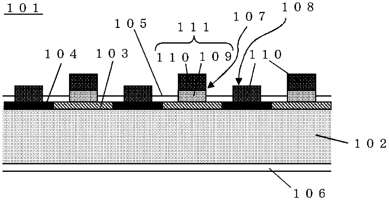
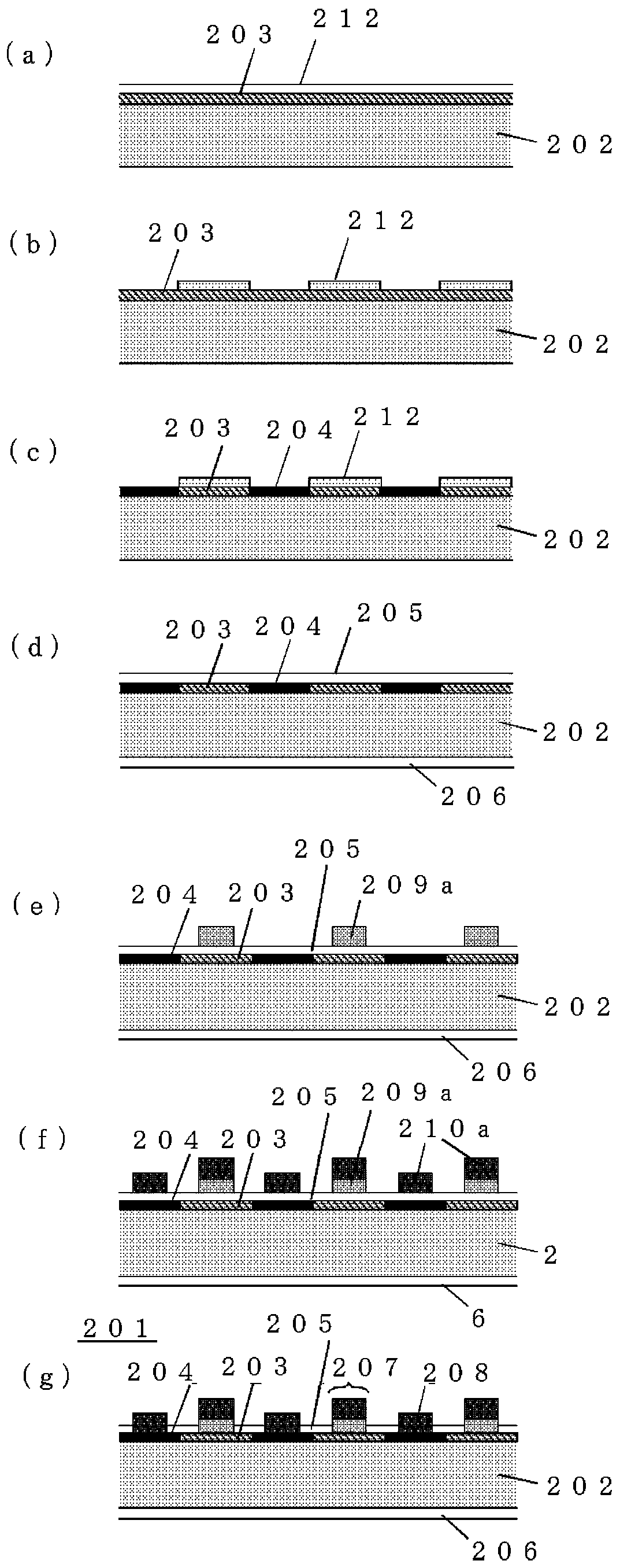
[0075] Initially, in a phosphorus-doped n-type as-cut silicon substrate with a square thickness of 150 mm, a thickness of 200 μm, and a resistivity of 1 Ω·cm, the damaged layer was removed by heating concentrated potassium hydroxide solution, and then heated in 5% potassium hydroxide at 80 ° C. Immerse in the solution for 20 minutes to form an irregular pyramid-like texture, and then wash in a hydrochloric acid / hydrogen peroxide mixed solution.
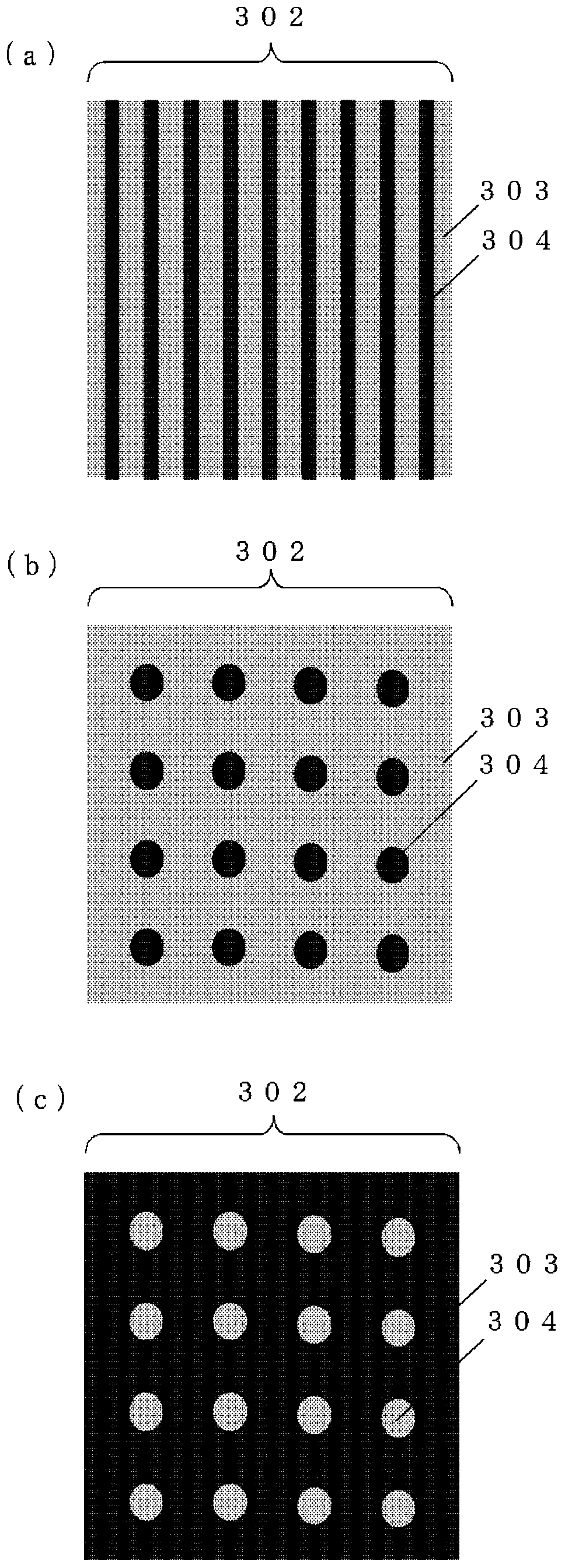
[0076] Next, the mixture of boron compound and binder is spin-coated on the back of the substrate, and boron is diffused by heat treatment at 1000°C for 30 minutes to form a p-type region, and then oxidation heat treatment is continued at 1000°C for 2 hours.
[0077] After the heat treatment, the oxide film at the position where the n-type region is formed on the rear surface of the substrate is removed linearly by irradiation with laser light having a wavelength of 532 nm.
[0078] Next, a set of two substrates with their light recei...
Embodiment 2
[0085] Operate with the same procedure as in Example 1 until a passivation film and an anti-reflection film are formed. On the obtained crystalline silicon substrate, by screen printing, mix a mixture of aluminum powder and glass frit and an organic binder to obtain The aluminum paste is coated on the p-type region and dried at 200°C for 1 minute.
[0086] Next, by screen printing, a silver paste to which no group III elements were added was applied to the dry body of the n-type region and the aluminum paste formed on the p-type region, dried at 200°C for 1 minute, and then subjected to 800°C, 3 The second heat treatment sinters the silver paste to obtain solar cells.
[0087] Finally, the output characteristics of the solar cell were measured using simulated sunlight of a xenon lamp light source type.
PUM
| Property | Measurement | Unit |
|---|---|---|
| thickness | aaaaa | aaaaa |
| electrical resistivity | aaaaa | aaaaa |
| thickness | aaaaa | aaaaa |
Abstract
Description
Claims
Application Information
 - R&D
- Intellectual Property
- Life Sciences
- Materials
- Tech Scout
- Unparalleled Data Quality
- Higher Quality Content
- 60% Fewer Hallucinations
Browse by: Latest US Patents, China's latest patents, Technical Efficacy Thesaurus, Application Domain, Technology Topic, Popular Technical Reports.
© 2025 PatSnap. All rights reserved.Legal|Privacy policy|Modern Slavery Act Transparency Statement|Sitemap|About US| Contact US: help@patsnap.com


