Self-excitation storable photoconductive device and preparation method thereof

A storage type, photoconductive technology, applied in the field of materials, to achieve the effects of high photoelectric efficiency, simple structure and high external quantum efficiency

Active Publication Date: 2020-02-21
SUZHOU UNIV OF SCI & TECH
View PDF3 Cites 3 Cited by
  • Summary
  • Abstract
  • Description
  • Claims
  • Application Information

AI Technical Summary

Problems solved by technology

The current van der Waals heterojunctions are almost all composed of two-dimensional P-type and N-type materials. Other two-dimensional systems, such as two-dimensional electron gas, have attracted widespread attention due to their exotic physical properties, but currently No van der Waals heterojunctions have been reported for electron gas

Method used


Image

  • Self-excitation storable photoconductive device and preparation method thereof
  • Self-excitation storable photoconductive device and preparation method thereof
  • Self-excitation storable photoconductive device and preparation method thereof

Examples


Embodiment 1

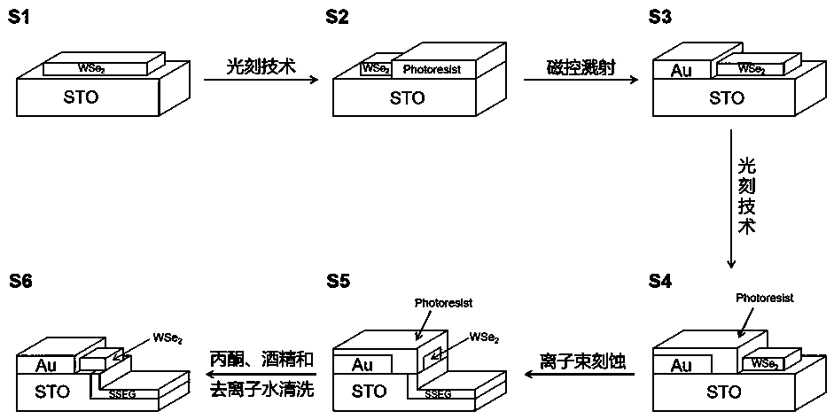
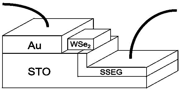
[0024] See attached figure 1 , which is the WSe provided by this example 2 Schematic diagram of the PN junction preparation process of / SSEG; the specific steps are:

[0025] S1: Few-layer WSe was bonded with adhesive tape 2 Flakes from monolithic WSe 2 transferred onto the surface of a single crystal STO substrate, and the obtained sample structure is shown in Figure S1;

[0026] S2: On one side of the sample, the WSe 2 The surface of 2 / 3 of the area and the STO substrate on this side are covered with photoresist, and the rest is exposed. The obtained sample structure is shown in Figure S2;

[0027] S3: Magnetron sputtering technology is used to deposit gold on the surface of the sample obtained in the previous step, and then the photoresist is removed with acetone, the exposed area in Figure S2 is covered by gold, and the rest is WSe 2 In the exposed state, the obtained sample structure is shown in Figure S3;

[0028] S4: Using photolithography again to cover WSe on on...


PUM

PropertyMeasurementUnit
external quantum efficiencyaaaaaaaaaa

Abstract

The invention discloses a self-excitation storable photoconductive device and a preparation method thereof. According to the invention, a single crystal STO substrate is used as an insulating oxide, and after ion beam bombardment, a nano conductive thin layer, namely surface electron gas SSEG, is formed on the surface layer of the single crystal STO substrate, and an N-type semiconductor is formed; WSe2 is a P-type two-dimensional semiconductor material, layers are combined together through Van der Waals force to form tungsten diselenide and strontium titanate surface electron gas and PN junctions thereof; the structure is simple, the photoelectric efficiency is high, storage property can be achieved, storage of photo-generated electron hole pairs can be achieved, and photo-generated carriers with the infinite service life are obtained; the working process is self-excited, the external quantum efficiency is high, the structure is simple, and the device can be applied to the field of nano energy devices.

Description

technical field [0001] The invention belongs to the technical field of materials, and in particular relates to a storable photoconductive device. Background technique [0002] Photovoltaic effect and photoconductive effect often occur when light is incident on the PN junction. High-efficiency optoelectronic devices often have excellent external quantum efficiency, and the rapid recombination of photogenerated electron-hole pairs greatly shortens the lifetime of carriers, thereby limiting the external quantum efficiency of optoelectronic devices. In order to obtain excellent optoelectronic devices, researchers have tried various strategies, such as using novel P-type and N-type semiconductor materials or designing new functional interfaces. At present, the improvement of external quantum efficiency is mainly achieved by improving the absorption of photons by devices, while there are relatively few studies on improving the lifetime of carriers. In recent years, the van der W...

Claims


Application Information

Patent Timeline
Patent Type & Authority Applications(China)
IPC IPC(8): H01L31/18H01L31/032H01L31/0749
CPCH01L31/032H01L31/0322H01L31/0749H01L31/18Y02E10/541Y02P70/50
Inventor 姜昱丞贺安鹏
Owner SUZHOU UNIV OF SCI & TECH
Why Eureka
Try Eureka