
Silicon carbide MOSFET module packaging structure and manufacturing method

A packaging structure and silicon carbide technology, which is applied in semiconductor/solid-state device manufacturing, semiconductor/solid-state device parts, semiconductor devices, etc., can solve problems such as not fully utilizing the advantages of silicon carbide power devices, and achieve high temperature resistance. The effect of improving heat dissipation efficiency

Active Publication Date: 2020-02-25
BEIJING UNIV OF TECH
View PDF5 Cites 7 Cited by
  • Summary
  • Abstract
  • Description
  • Claims
  • Application Information

AI Technical Summary

Problems solved by technology

[0006] Although the above inventions have realized the good application of silicon carbide power modules at higher frequencies to a certain extent, they have not fully utilized the advantages of silicon carbide power devices over silicon-based power devices under high-temperature application conditions.

Method used


Image

  • Silicon carbide MOSFET module packaging structure and manufacturing method
  • Silicon carbide MOSFET module packaging structure and manufacturing method
  • Silicon carbide MOSFET module packaging structure and manufacturing method

Examples


Embodiment Construction

[0048] In order to make the present invention more obvious and understandable, the specific implementation manners of the present invention will be described in detail below in conjunction with the accompanying drawings. For convenience of description, the components in the structures in the drawings of the embodiments are not scaled according to the normal scale, so they do not represent the actual relative sizes of the structures in the embodiments.

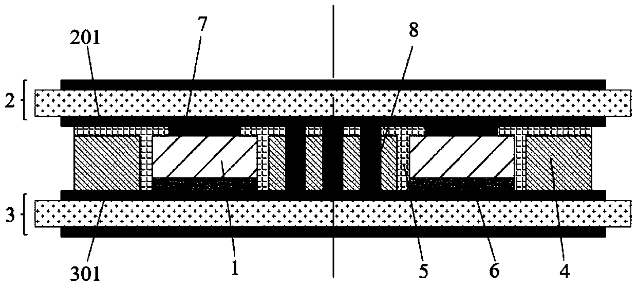
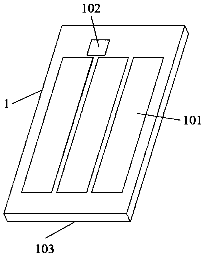
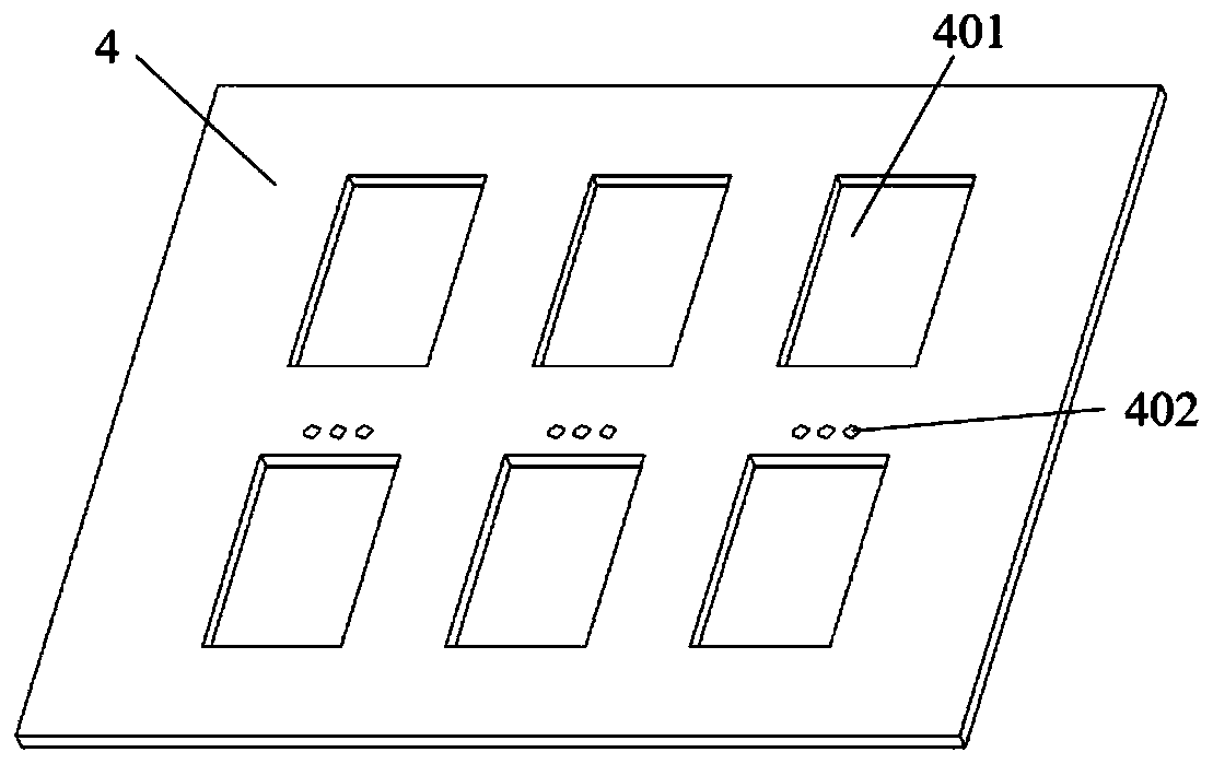
[0049] Such as figure 1 As shown, the present invention discloses a packaging structure of a silicon carbide MOSFET module, which consists of a silicon carbide MOSFET chip (1) with an embedded SBD, an upper DBC substrate (2), a lower DBC substrate (3), and a ceramic adapter plate (4 ), silicon oxide dielectric filling layer (5), nano-silver solder paste (6), rewiring layer (7), via conductive metal (8), positive terminal (9a), negative terminal (9d), gate-level terminal (9b) and common terminal (9c). The silicon carbide MOSFE...


PUM


Abstract

The invention discloses a silicon carbide MOSFET module packaging structure and a manufacturing method. The silicon carbide MOSFET module packaging structure is composed of a silicon carbide MOSFET chip, an upper DBC substrate, a lower DBC substrate, a ceramic adapter plate, a silicon oxide dielectric filling layer, nano-silver soldering paste, a rewiring layer, via hole conductive metal and powerterminals. The silicon carbide MOSFET chip is connected with the lower DBC substrate through the nano-silver soldering paste. And meanwhile, a rectangular frame is manufactured on the ceramic adapterplate, and the silicon carbide MOSFET chip is embedded into the ceramic adapter plate by filling a dielectric material. The upper surfaces of the chip and the adapter plate are coated with conductivemetal layers, the upper surface and the lower surface of the ceramic adapter plate are mutually connected with the upper DBC substrate and the lower DBC substrate respectively, and the power terminals are led out from the conductive copper-clad layers of the upper DBC substrate and the lower DBC substrate respectively. Thus, high-temperature packaging of the silicon carbide MOSFET module can be realized, double-sided heat dissipation can be realized, and the heat dissipation efficiency is improved. A planar interconnection mode is adopted to replace lead bonding, so that the parasitic inductance of the module is reduced.

Description

technical field [0001] The invention relates to the technical field of packaging of power electronic devices, in particular to a packaging structure and a manufacturing method of a silicon carbide power module. Background technique [0002] The development of power electronics technology is always moving towards higher efficiency, higher power density and higher integration. Nowadays, compared with traditional silicon-based power semiconductor devices, wide-bandgap power semiconductor power devices have smaller volume, lower conduction loss, higher breakdown voltage, higher thermal conductivity and higher working efficiency. Therefore, wide bandgap power semiconductor devices are suitable for high-voltage, high-temperature, and high-frequency application scenarios, which are in line with the development trend of power electronics technology. It can be said that wide bandgap power semiconductor devices determine the pace of development of today's power electronics technology...

Claims


Application Information

Patent Timeline
Patent Type & Authority Applications(China)
IPC IPC(8): H01L25/07H01L23/367H01L23/31H01L21/50
CPCH01L25/072H01L23/367H01L23/3107H01L21/50H01L2224/33181H01L23/5389H01L23/5384H01L23/3735H01L23/15H01L23/49844H01L2224/32227H01L2224/3303H01L2224/29294H01L2224/29339H01L2224/293H01L2224/2732H01L2224/83192H01L24/27H01L24/29H01L24/32H01L24/33H01L24/83H01L2924/00014H01L2924/014H01L24/19H01L24/24H01L29/1608H01L2224/24245H01L2224/32245H01L2924/01047H01L2924/30107
Inventor 秦飞赵帅代岩伟陈沛安彤
Owner BEIJING UNIV OF TECH
Learn More