Semiconductor device structure and preparation method thereof

A device structure, semiconductor technology, applied in the direction of semiconductor devices, electrical solid devices, electrical components, etc., can solve the problems that the performance of transistors cannot meet the requirements, the conduction current drops, etc., to improve the short channel effect, increase the channel area, The effect of increasing the width

Pending Publication Date: 2020-03-13
CHANGXIN MEMORY TECH INC
View PDF0 Cites 3 Cited by
  • Summary
  • Abstract
  • Description
  • Claims
  • Application Information

AI Technical Summary

Problems solved by technology

[0006] In view of the shortcomings of the prior art described above, the purpose of the present invention is to provide a semiconductor device structure and its preparation method, which are used to solve the problems of the transistor performance that is difficult to meet the demand and the driving voltage and on-current drop in the prior art.

Method used


Image

  • Semiconductor device structure and preparation method thereof
  • Semiconductor device structure and preparation method thereof
  • Semiconductor device structure and preparation method thereof

Examples


preparation example Construction

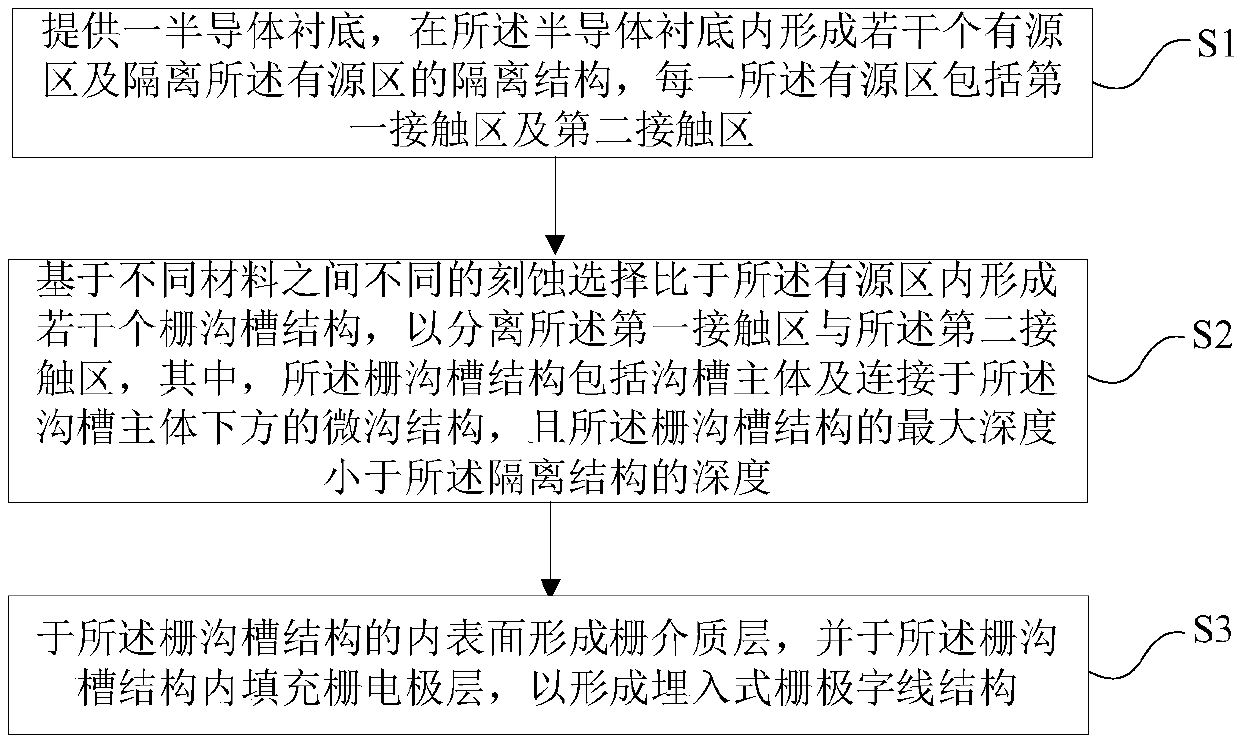
[0078] Such as figure 1 Shown, the preparation method of a kind of semiconductor device structure of the present invention, described preparation method comprises the following steps:

[0079] 1) A semiconductor substrate is provided, and several active regions and isolation structures for isolating the active regions are formed in the semiconductor substrate, and each active region includes a first contact region and a second contact region ;

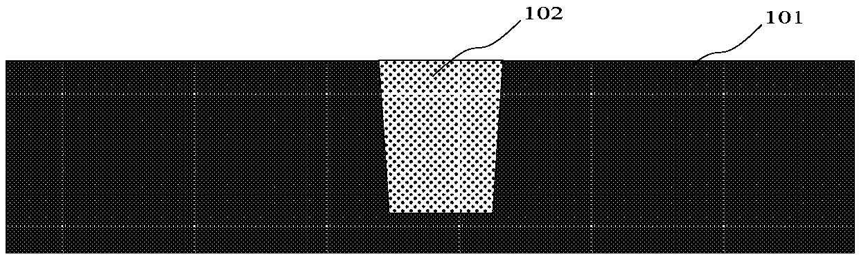
[0080] 2) Based on different etching selectivity ratios between different materials, several gate trench structures are formed in the active region to separate the first contact region and the second contact region, wherein the gate trench The trench structure includes a trench body and a micro-trench structure connected under the trench body, and the maximum depth of the gate trench structure is smaller than the depth of the isolation structure; and

[0081] 3) A gate dielectric layer is formed on the inner surface of the gate trenc...

Embodiment 1

[0103] Such as Figure 8-19 As shown, this embodiment provides a method for forming the gate trench structure 103, and the forming steps specifically include:

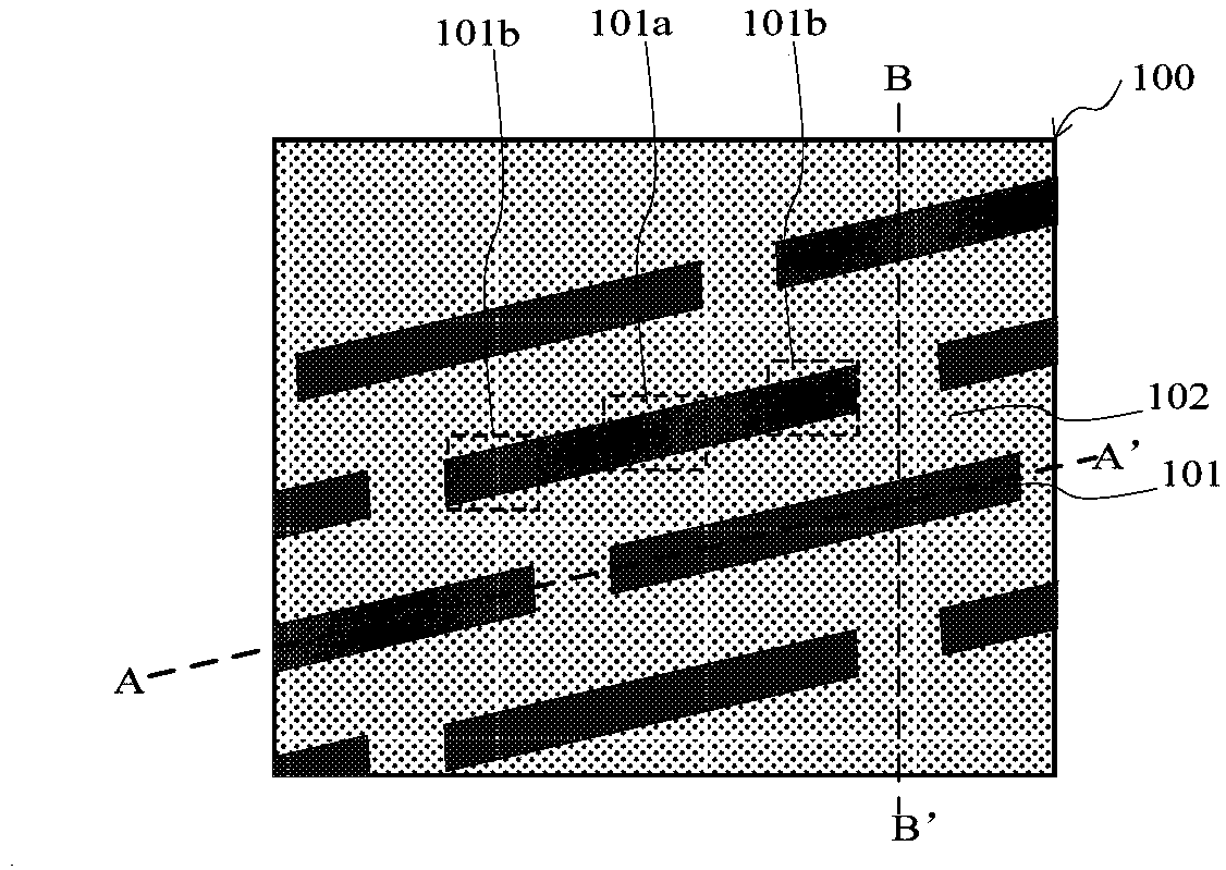
[0104] Such as Figure 8-10 As shown, step 2-1) is performed to form an etching mask layer 112 on the semiconductor substrate 100, and several gate trench windows 106 are formed on the etching mask layer. The window 106 exposes the active region 101 and defines the position of the gate trench structure 103; specifically, first defines the position of the gate trench structure 103 in the active region 101, in an example In each of the active regions 101, two gate trench windows 106 are correspondingly formed, and are located between the adjacent first contact regions 101a and the second contact regions 101b.

[0105] As an example, the etching mask layer 112 includes a hard mask layer 104 and a photoresist layer 105 sequentially formed on the semiconductor substrate 100, and the thickness of the hard mask layer 501 is...

Embodiment 2

[0116] Such as Figure 20-39 As shown, this embodiment provides another method for forming the gate trench structure, and the forming steps specifically include:

[0117] Such as Figure 20-22 As shown, step 2-1) is performed to form a hard mask layer 201 on the semiconductor substrate 100, and several etching windows 203 are formed on the hard mask layer, and the etching windows 203 expose The active region 101 defines the position of the gate trench structure 103; specifically, first defines the position of the gate trench structure 103 in the active region 101, in an example, each Two gate trench windows 106 are correspondingly formed on the active region 101, and are located between the adjacent first contact region 101a and the second contact region 101b.

[0118] As an example, the hard mask layer 201 is formed based on a photoresist layer 202, so as to etch down the photoresist layer 202 to form the gate trench structure 103, wherein the thickness of the hard mask lay...


PUM

PropertyMeasurementUnit
depthaaaaaaaaaa
widthaaaaaaaaaa
depthaaaaaaaaaa

Abstract

The invention provides a semiconductor device structure and a preparation method thereof, and the preparation method comprises the steps of providing a semiconductor substrate, and forming a pluralityof active regions and an isolation structure for isolating the active regions, wherein each active region comprises a first contact region and a second contact region; forming a plurality of gate trench structures in the active regions based on different etching selection ratios among different materials so as to separate the first contact region from the second contact region, wherein each gatetrench structure comprises a trench main body and a micro-trench structure, and the maximum depth of each gate trench structure is smaller than the depth of the isolation structure; and forming a gatedielectric layer on the inner surfaces of the gate trench structures, and filling a gate electrode layer in the gate trench structures to form an embedded gate word line structure. According to the invention, a special micro-channel structure is formed through different etching selection ratios among different materials, the preparation process is simplified, the preparation precision is improved, the channel area is increased on the basis of keeping the size of an original device, the width of a transmission channel can be further increased, and the device performance of a field effect transistor is improved.

Description

technical field [0001] The invention belongs to the technical field of integrated circuit manufacturing, and in particular relates to a semiconductor device structure and a preparation method thereof. Background technique [0002] With the evolution of semiconductor manufacturing process and the continuous shrinking of the feature size of semiconductor devices, for field effect transistors, due to the short channel effect, large sub-threshold current and gate leakage, it is difficult for transistors to meet the requirements of device performance. Now more and more attention is focused on the Fin Field Effect Transistor (Fin FET). [0003] Transistors are used in many different types of integrated circuits. The common ones are: logic devices, storage devices and analog circuits. Among them, storage devices account for a considerable proportion of integrated circuit products. The basic structure of memory is a transistor plus a capacitor structure. The transistors used are bu...

Claims


Application Information

Patent Timeline
Patent Type & Authority Applications(China)
IPC IPC(8): H01L27/11521H01L27/11526H01L27/11568H01L27/11573H01L21/28H01L29/10H01L29/423
CPCH01L29/1033H01L29/401H01L29/4236H10B41/30H10B41/40H10B43/30H10B43/40
Inventor 不公告发明人
Owner CHANGXIN MEMORY TECH INC
Why Eureka
Try Eureka