

Silicon wafer with silicon oxide film on surface and preparation method
A technology of silicon oxide and thin film, which is applied in semiconductor/solid-state device manufacturing, electrical components, circuits, etc., can solve problems such as difficult insulating layers, reduce reaction temperature, prevent adverse effects, and expand application prospects
- Summary
- Abstract
- Description
- Claims
- Application Information
AI Technical Summary
Problems solved by technology
Method used
Image

Examples
Embodiment 1
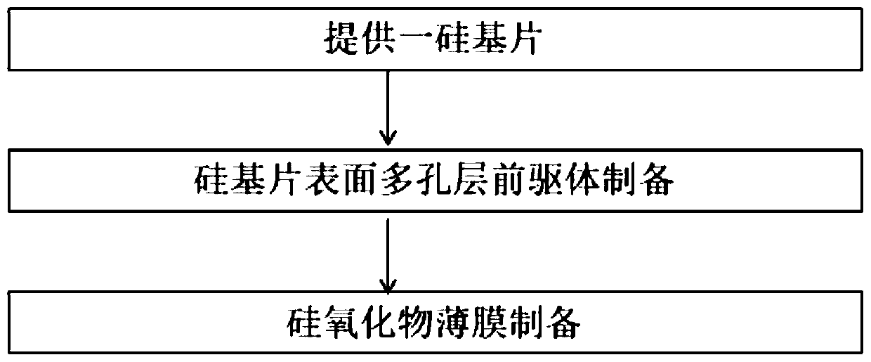
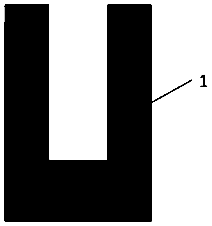
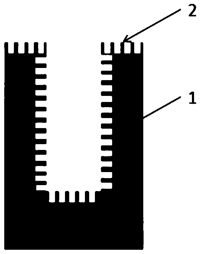
[0044] see figure 1 , Figure 2a to Figure 2c Shown, the invention provides a kind of preparation method of the silicon chip that the surface has silicon oxide thin film, it comprises the steps:
[0045] A1: Provide a silicon substrate 1, the surface of the silicon substrate 1 is provided with vertical blind holes or through holes, and the aspect ratio of the blind holes or through holes is 1:1~1:10;
[0046]A2: Preparation of the precursor of the porous layer on the surface of the silicon substrate: cover the other surface of the silicon substrate that does not need to be etched with polyimide tape, and then place the silicon substrate 1 in the etching solution, The outer surface in contact with the etching solution provides fluoride ions, and at room temperature, the surface of the silicon substrate 1 and the walls of the blind holes are etched by electrolysis to form a porous layer 2. In this embodiment, the composition of the etching solution is Ethanol and fluorine-cont...
Embodiment 2
[0059] This embodiment provides a method for preparing a silicon wafer with a silicon oxide film on the surface. The aspect ratio of the blind hole is selected to be 1:5, and the resistivity is 10. -2 Ω silicon substrate; the specific steps are as follows:
[0060] Step 1: Under the condition of 25°C, use acetone, alcohol and deionized water to ultrasonically clean the silicon wafer for 5 minutes respectively, take it out and dry it for later use;
[0061] Step 2: Prepare an etching solution. In this embodiment, the etching solution is composed of ethanol and a fluorine-containing reagent, wherein the fluorine-containing reagent is preferably a hydrofluoric acid reagent. Add 250 mL of 95% pure absolute ethanol into a polytetrafluoroethylene container, then add 50 mL of 40% hydrofluoric acid solution under magnetic stirring, stir for 20 minutes and let stand to obtain a clear solution.
[0062] Step 3: After the silicon substrate cleaned in step 1 is covered with polyimide tap...
Embodiment 3
[0067] This embodiment provides a method for preparing a silicon wafer with a silicon oxide film on the surface, using a silicon substrate with a blind hole aspect ratio of 1:10 and a resistivity of 20Ω; the specific steps are as follows:
[0068] Step 1: Under the condition of 25°C, use acetone, alcohol and deionized water to ultrasonically clean the silicon wafer for 5 minutes respectively, take it out and dry it for later use;
[0069] Step 2: Prepare an etching solution. In this embodiment, the etching solution is composed of ethanol and a fluorine-containing reagent, wherein the fluorine-containing reagent is preferably a hydrofluoric acid reagent. Add 250 mL of 95% pure absolute ethanol into a polytetrafluoroethylene container, then add 50 mL of 40% hydrofluoric acid solution under magnetic stirring, stir for 20 minutes and let stand to obtain a clear solution.
[0070] Step 3: After the silicon substrate cleaned in step 1 is covered with polyimide tape, the part of the ...
PUM
 Abstract
Description
Claims
Application Information