A kind of through-hole electroplating method of printed circuit board

A printed circuit board and through-hole electroplating technology, which is applied in the field of printed circuit boards, can solve problems such as unfavorable human health, and achieve the effects of fast electron migration, enhanced throwing ability, and good dispersion ability

Active Publication Date: 2021-10-26
UNIV OF ELECTRONICS SCI & TECH OF CHINA +1
View PDF10 Cites 2 Cited by
  • Summary
  • Abstract
  • Description
  • Claims
  • Application Information

AI Technical Summary

Problems solved by technology

However, it uses highly toxic organic solvents such as tetrahydrofuran, which is not conducive to human health

Method used


Image

  • A kind of through-hole electroplating method of printed circuit board
  • A kind of through-hole electroplating method of printed circuit board
  • A kind of through-hole electroplating method of printed circuit board

Examples


Embodiment Construction

[0049] The principles and features of the present invention are described below in conjunction with the accompanying drawings, and the examples given are only used to explain the present invention, and are not intended to limit the scope of the present invention.

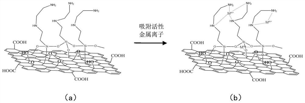
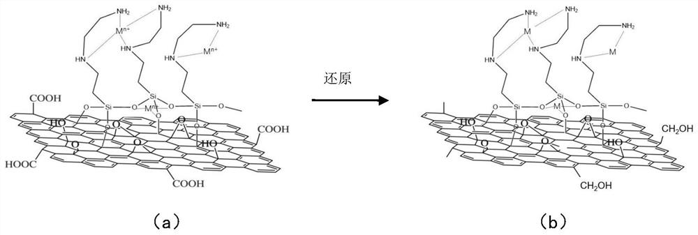
[0050] like Figure 1-6 As shown, a method for through-hole plating of a printed circuit board provided in an embodiment of the present invention includes the following steps:

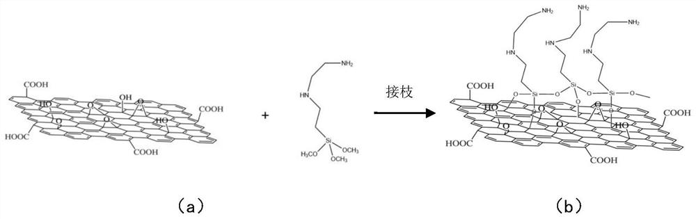
[0051] Step 1: Make graphene oxide graft γ-aminoethylaminopropyltrimethoxysilane to obtain product A, such as figure 1 shown, where figure 1 In (a), the left side is the structural formula of graphene oxide, and the right side is the structural formula of γ-aminoethylaminopropyltrimethoxysilane, figure 1 (b) is the structural formula of the product A after grafting;

[0052] Dissolve 50mg of γ-aminoethylaminopropyltrimethoxysilane and 100mg of graphene oxide in 100mL of ethanol solution, then stir and react at 65°C at 100rpm for 10h, then...


PUM

PropertyMeasurementUnit
concentrationaaaaaaaaaa

Abstract

The invention relates to a through-hole electroplating method of a printed circuit board, comprising the following steps: grafting graphene oxide with γ-aminoethylaminopropyltrimethoxysilane to obtain a product A; making the product A adsorb active metal ions, The product B is obtained; the product B is physically adsorbed to the surface of the insulating substrate of the through-hole wall of the printed circuit board to form an adsorption layer; the adsorption layer is converted into a conductive layer through a chemical reduction process; the through-hole wall with a conductive layer is electroplated A metal layer is formed. In the present invention, graphene oxide is selected and grafted with γ-aminoethylaminopropyltrimethoxysilane. Due to the formation of high-density oxygen bond functional sites at the grafting interface, the adsorption capacity for active metal ions is effectively improved, and the conductive layer The ethylenediamine groups on the surface can effectively improve the ability to capture copper ions in the solution during the electroplating process, accelerate the mass transfer of copper ions, and facilitate the accelerated deposition of copper plating in the holes, thereby greatly enhancing the uniformity of the plating solution. Plating ability.

Description

technical field [0001] The invention belongs to the field of printed circuit boards, and in particular relates to a through-hole electroplating method for printed circuit boards. Background technique [0002] After the printed circuit board is drilled, hole metallization is required to achieve interconnection between layers. Hole metallization consists of two steps, first forming a conductive layer on the hole wall, and then thickening it by electroplating. Graphene is a two-dimensional material with ultrahigh electrical conductivity. At present, the industry has begun to try to use graphene as a conductive layer in the metallization process. [0003] However, if the conductive layer does not contain metal or metal particles, it is difficult to directly deposit the coating on the non-metallic conductive layer. Usually, it is necessary to use the original metal as the starting point for lateral growth, but the uniformity of the thickness of the coating formed in this way P...

Claims


Application Information

Patent Timeline
Patent Type & Authority Patents(China)
IPC IPC(8): C25D7/04C25D5/56C25D5/18C25D3/38
CPCC25D3/38C25D5/18C25D5/56C25D7/04
Inventor 陈苑明王英杰李清华何为王翀王守绪周国云王青云艾克华胡志强
Owner UNIV OF ELECTRONICS SCI & TECH OF CHINA
Why Eureka
Try Eureka