Tunneling Field Effect Transistor and Manufacturing Method
A tunneling field effect and transistor technology, applied in the field of microelectronics, can solve problems such as increased power consumption, device performance degradation, and reduced reliability
- Summary
- Abstract
- Description
- Claims
- Application Information
AI Technical Summary
Problems solved by technology
Method used
Image
Examples
Embodiment 1
[0061] Embodiment 1: Fabricate a tunneling field effect transistor with one gate sensing plate and one drain sensing plate.
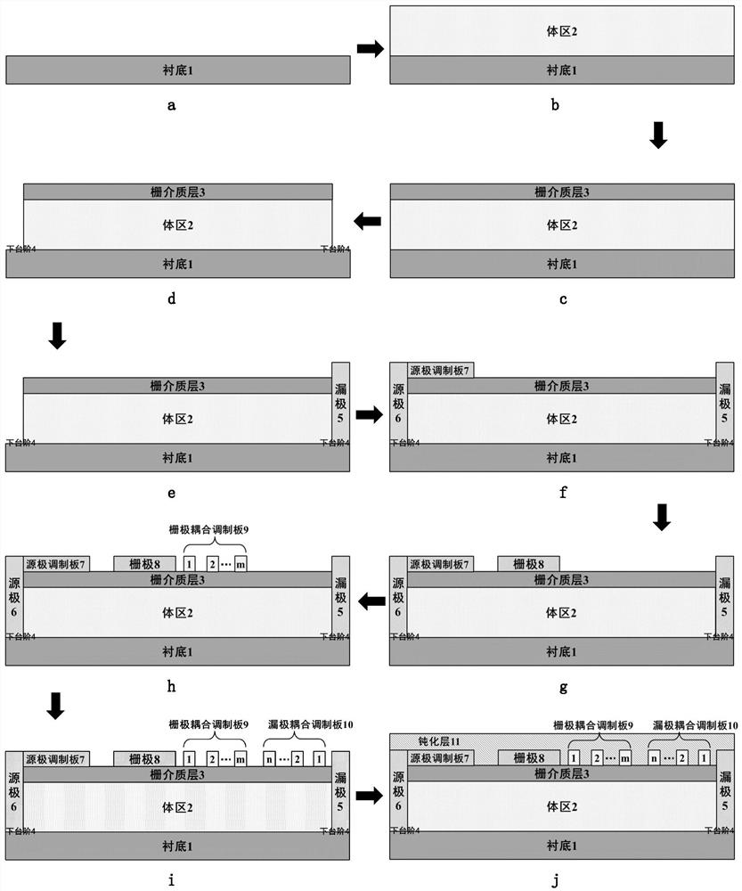
[0062] Step 1. Select silicon semiconductor material as substrate 1, such as image 3 a.
[0063] Step 2. Fabricate the body region 2 on the silicon substrate 1, such as image 3 b.
[0064] A silicon semiconductor material with a thickness of 5 nm is epitaxially grown on a silicon substrate 1 using molecular beam epitaxy technology to form a bulk region 2, wherein the process conditions used for the epitaxy are: the degree of vacuum is less than or equal to 1.0×10 -10 mbar, the RF power is 150W, and the reactant uses high-purity silicon source.
[0065] Step 3. Make gate dielectric layer 3, such as image 3 c.
[0066] A layer of SiN insulating dielectric material with a thickness of 0.5nm is deposited on the upper part of the body region 2 using plasma-enhanced chemical vapor deposition technology, wherein the process conditions for depositing th...
Embodiment 2
[0081] Embodiment 2: Making a Tunneling Field Effect Transistor with 2 Gate Sensing Plates and 2 Drain Sensing Plates
[0082] Step 1. Select InN semiconductor material as substrate 1, such as image 3 a.
[0083] Step 2. Fabricate the body region 2 on the InN substrate 1, such as image 3 b.
[0084] Using molecular beam epitaxy on an InN substrate 1, the vacuum degree is less than or equal to 1.0×10 -10 mbar, the RF power is 150W, and the reactant uses high-purity In source, N 2 The body region 2 is formed by epitaxially epitaxially InN semiconductor material with a thickness of 25 nm under certain process conditions.
[0085] Step 3. Make gate dielectric layer 3, such as image 3 c.
[0086] Use plasma-enhanced chemical vapor deposition technology in the upper part of the body region 2 in the gas NH 3 , N 2 and SiH 4 , the gas flow rate is 2.5sccm, 950sccm and 250sccm, the temperature is 300°C, the RF power is 25W, and the pressure is 950mTorr, a layer of SiN insul...
Embodiment 3
[0105] Embodiment 3: Fabricate a tunneling field effect transistor with three gate sensing plates and three drain sensing plates.
[0106] Step A. select Ge semiconductor material as substrate 1, such as image 3 a.
[0107] Step B. Fabricate body region 2 on Ge substrate 1, such as image 3 b.
[0108] On the Ge substrate 1, a germanium semiconductor material with a thickness of 50nm is epitaxed by using molecular beam epitaxy technology to form the body region 2, wherein the process conditions used for the epitaxy are as follows:
[0109] Vacuum degree is less than or equal to 1.0×10 -10 mbar,
[0110] RF power is 150W,
[0111] The reactant adopts high-purity germanium source.
[0112] Step C. Make gate dielectric layer 3, such as image 3 c.
[0113] A layer of SiN insulating dielectric material with a thickness of 40nm is deposited on the upper part of the body region 2 using plasma enhanced chemical vapor deposition technology, wherein the process conditions for ...
PUM
| Property | Measurement | Unit |
|---|---|---|
| width | aaaaa | aaaaa |
| thickness | aaaaa | aaaaa |
| thickness | aaaaa | aaaaa |
Abstract
Description
Claims
Application Information


