LED assembly, quantum dot LED light-emitting part, quantum dot LED packaging structure and display equipment

A technology for LED components and LED packaging, applied in electrical components, semiconductor devices, circuits, etc., can solve problems such as the decline of quantum dot light conversion efficiency, quenching and blackening of quantum dot packaging layers, and achieve a simple and fast product manufacturing process. Effect

Active Publication Date: 2020-04-28
NANJING TECH CORP LTD
View PDF9 Cites 1 Cited by
  • Summary
  • Abstract
  • Description
  • Claims
  • Application Information

AI Technical Summary

Problems solved by technology

This packaging solution has the advantage of being thinner and lighter, but the barrier layer with high water and oxygen barrier properties has no cost advantage, and the light conversion efficiency of quantum dots cured in the adhesive layer also inevitably leads to a decline
[0005] In addition, the more important defects in the existing technology are also concentrated in the problem of light quenching: the quantum dots close to the middle of the chip will first be quenched by the strong blue light of the chip, causing blackening, and continuously Deterioration, black absorbs blue light and heats up, resulting in quenching of the entire quantum dot encapsulation layer
If the diffusion layer is introduced into the diaphragm or close to the chip side, or scattering particles are added, it will cause a decrease in luminous efficiency, resulting in low brightness
For now, the above-mentioned technical contradictions cannot be effectively resolved in the prior art

Method used


Image

  • LED assembly, quantum dot LED light-emitting part, quantum dot LED packaging structure and display equipment
  • LED assembly, quantum dot LED light-emitting part, quantum dot LED packaging structure and display equipment
  • LED assembly, quantum dot LED light-emitting part, quantum dot LED packaging structure and display equipment

Examples


preparation example Construction

[0050] The application also provides a method for preparing an LED component, such as Figures 1 to 4 shown, including the following steps:

[0051] Provide LED chip 1;

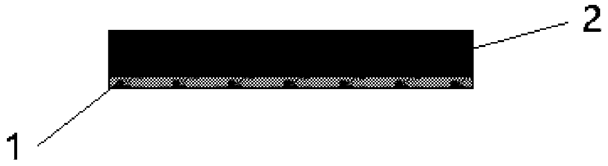
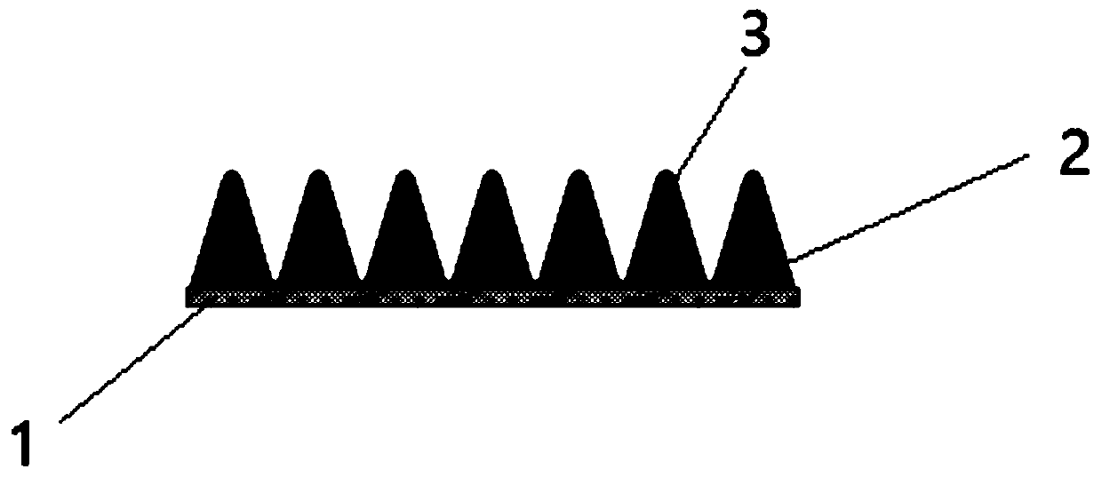
[0052] disposing an organic polymer or an inorganic substance on the surface of one side of the LED chip 1;

[0053] Etching the organic polymer or inorganic substance so that it has a porous structure 4;

[0054] Before and / or after the etching treatment, several protrusions 3 are formed on the surface of the organic polymer or inorganic substance through a surface treatment process to obtain a light-transmitting quantum dot accommodation structure.

[0055] It is worth mentioning that the above method uses etching to form a porous structure 4 to construct a light-transmitting quantum dot accommodation structure with high light transmittance, so that the quantum dots can be arranged in a specific shape in a three-dimensional space. The multiple refraction guide provided by the light prevents the quantum d...

Embodiment 1

[0079] see Figure 1~5 , take the LED chip 1, and coat a layer of polymethyl methacrylate on it to form a transparent organic polymer layer 2, the thickness of which is 100 μm, and then use nanoimprinting to carry out the surface structure of the organic polymer layer 2 chemical treatment to form regular protrusions 3 with a size of 65 μm and an adjacent spacing of 20 μm, and then use a solvent (including but not limited to ethyl acetate, toluene, etc.) to etch them to form a porous structure 4, Finally, hydrophobic treatment is performed on the porous structure 4 .

[0080] see Figure 7-10 , cut the LED assembly obtained above according to a certain size to obtain microchips 9 . Place the microchip 9 in the middle of the LED bracket 7, and drip the CdSe quantum dot solution to it, wherein the viscosity of the selected quantum dot solution is 48cps; after ensuring that an appropriate amount of the quantum dot solution penetrates into the porous structure 4, dry it to make t...

Embodiment 2

[0082] Take the LED chip 1, coat it with a layer of polydimethylsiloxane to form a transparent organic polymer layer 2, the thickness of which is 100 μm, and then use nanoimprinting to carry out the surface structure of the organic polymer layer 2 Chemical treatment to form regular protrusions 3 with a size of 40 μm and an adjacent spacing of 10 μm, and then use a solvent (including but not limited to ethyl acetate, toluene, etc.) to etch them to form a porous structure 4 .

[0083]The LED assembly obtained above is cut according to a certain size to obtain a microchip 9 . Microchip 9 is placed in the middle of LED support 7, and it is carried out the instillation of CdSe quantum dot solution (quantum dot solution identical with embodiment 1), wherein the quantum dot solution viscosity of selection is 10cps; When guaranteeing an amount of quantum dot After the solution penetrates into the porous structure 4 , it is dried to evaporate the solvent contained in the quantum dot so...


PUM

PropertyMeasurementUnit
heightaaaaaaaaaa

Abstract

The invention relates to an LED assembly, a quantum dot LED light-emitting part, a quantum dot LED packaging structure and display equipment. The LED assembly comprises an LED chip, and a light-transmitting quantum dot containing structure with a plurality of protrusions in the surface is arranged on one side face of the LED chip. The light-transmitting quantum dot containing structure is a porousstructure; and the light-transmitting quantum dot containing structure is made of an organic polymer or an inorganic substance. A material capable of forming a porous structure through etching treatment is utilized to construct the light-transmitting quantum dot containing structure with high light transmittance by taking a quantum dot as a light source, so that the quantum dot can be arranged ina specific form in a three-dimensional space, and in addition, by combining a multiple refraction guide path provided for light, the quantum dot in the whole region is prevented from being systematically quenched due to quenching blackening caused by excessive blue light irradiation on the quantum dot in a local range; the blue light absorption rate of the quantum dots is effectively improved, the actual usage amount of the quantum dots can be effectively reduced under the same brightness while the high light conversion rate is achieved, and therefore the cost is reduced.

Description

technical field [0001] The invention belongs to the technical field of LED manufacturing, and relates to an LED assembly and a related quantum dot LED device derived therefrom, in particular to an LED assembly, a quantum dot LED light-emitting part, a quantum dot LED packaging structure and a display device. Background technique [0002] Quantum dots are semiconductor nanostructures that can confine excitons in three spatial directions. By applying an electric field or light to the quantum dots, the quantum dots can emit photons to the outside. In real scenarios, water, oxygen and heat damage are important factors restricting the application of quantum dots. To address this problem, the prior art provides a variety of related technical solutions as follows: [0003] The Chinese patent with publication number CN109755357A discloses a quantum dot LED packaging structure and packaging method, in order to effectively protect the quantum dot layer by setting a heat insulating l...

Claims


Application Information

Patent Timeline
Patent Type & Authority Applications(China)
IPC IPC(8): H01L33/50H01L33/58H01L33/56H01L33/54
CPCH01L33/505H01L33/54H01L33/56H01L33/58H01L2933/0041
Inventor 余世荣康永印罗飞
Owner NANJING TECH CORP LTD
Why Eureka
Try Eureka