Ferroelectric polarization regulated artificial synaptic device and preparation method thereof
A synaptic device and ferroelectric technology, applied in the field of artificial synaptic devices based on organic ferroelectric polarization regulation and their preparation, can solve the problems of poor repeatability and uniformity of memristors, limiting the development of memristors, etc. Achieve good fatigue characteristics, long life, improved stability and repeatability
- Summary
- Abstract
- Description
- Claims
- Application Information
AI Technical Summary
Problems solved by technology
Method used
Image
Examples
Embodiment 1
[0031] Prepare artificial synaptic devices based on organic ferroelectrics according to the following steps:
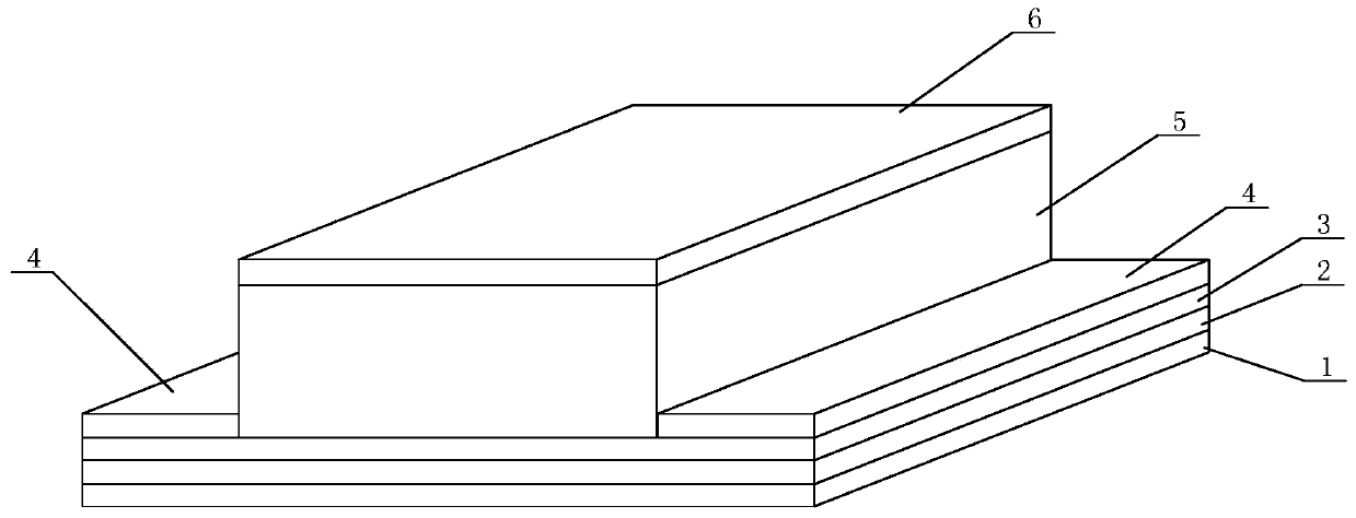
[0032] 1) Substrate selection: select heavily doped p-type silicon with a thickness of 0.5mm as substrate 1, and perform single-sided polishing
[0033] Light processing.
[0034] 2) Preparation of oxide dielectric layer: thermally oxidize 285nm silicon dioxide to SiO on the surface of p-type silicon 2 / Si's oxide layer 2.
[0035] 3) Two-dimensional semiconductor transfer preparation: use tape to transfer the MoS of transition metal chalcogenide 2 The crystal is removed mechanically and transferred to SiO 2 / Si on the oxide layer 2, its MoS 2 The thickness is three molecular layers.
[0036] 4) Preparation of metal source and drain electrodes: the electrode pattern is prepared by the ultraviolet lithography method, and then the metal electrode with 5nm chromium and 30nm gold as the source / drain electrode is prepared by thermal evaporation technology. 4, combined with the lift-...
Embodiment 2
[0046] Prepare artificial synaptic devices based on organic ferroelectrics according to the following steps:
[0047] 1) Substrate selection: Use heavily doped p-type silicon with a thickness of 0.5 mm as substrate 1, and perform single-sided polishing.
[0048] 2) Preparation of oxide dielectric layer: thermally oxidize 285nm silicon dioxide to SiO on the surface of p-type silicon 2 / Si's oxide layer 2.
[0049] 3) Two-dimensional semiconductor transfer preparation: tape the WSe of the transition metal chalcogenide 2 The crystal is removed mechanically and transferred to SiO 2 / Si on the oxide layer 2, its MoS 2 The thickness is five molecular layers.
[0050] 4) Preparation of metal source and drain electrodes: the electrode pattern is prepared by ultraviolet lithography, and then the metal electrode with 5nm chromium and 30nm gold is prepared by thermal evaporation technology, combined with the lift-off method, the source / drain electrode is stripped off the metal film 4 , A back ga...
PUM
| Property | Measurement | Unit |
|---|---|---|
| thickness | aaaaa | aaaaa |
| thickness | aaaaa | aaaaa |
| thickness | aaaaa | aaaaa |
Abstract
Description
Claims
Application Information


