Structure and method for improving thermal stability and reliability of ohmic contact of N polar surface GaN

A technology of ohmic contact and thermal stability, applied in the direction of electrical components, circuits, semiconductor devices, etc., can solve the problems of device performance degradation, ohmic contact characteristic deterioration, photolithography deviation, etc., to achieve high repeatability and reliability, reduce Effect of specific contact resistivity and improvement of thermal stability

Inactive Publication Date: 2020-05-08
SUN YAT SEN UNIV
View PDF3 Cites 0 Cited by
  • Summary
  • Abstract
  • Description
  • Claims
  • Application Information

AI Technical Summary

Problems solved by technology

[0003] 1. The density of dangling bonds on the surface of N-polar GaN is high, and a large amount of oxygen or hydroxide is adsorbed. During the annealing process, metal oxides will be formed with traditional metal electrode materials, which will increase the contact barrier between the metal and GaN, and deteriorate the ohmic contact. The quality of the material affects the reliability of the device (Wang Xianbin, Wang Yingli, Zhao Zhengping. Ohmic contact of Ti/Al/Ni/Au on N-polar GaN[J]. Materials Herald, 2017,31(04):14-16.)
[0004] 2. The combination metal of Ti/Al/Ni/Au is usually used to make the ohmic contact electrode, in which the metal Al reacts with GaN to form AlN in the high-temperature molten state. For GaN on the Ga polar surface, the interface between AlN and GaN will form a high Concentration of two-dimensional electron gas, which is beneficial to improve the ohmic characteristics of Ga-face GaN, but for N-face GaN, du

Method used


Image

  • Structure and method for improving thermal stability and reliability of ohmic contact of N polar surface GaN
  • Structure and method for improving thermal stability and reliability of ohmic contact of N polar surface GaN

Examples


Embodiment Construction

[0028] The present invention will be further described below in conjunction with the accompanying drawings. It should be noted that the following examples are based on the premise of this technical solution, and provide detailed implementation and specific operation process, but the protection scope of the present invention is not limited to the present invention. Example.

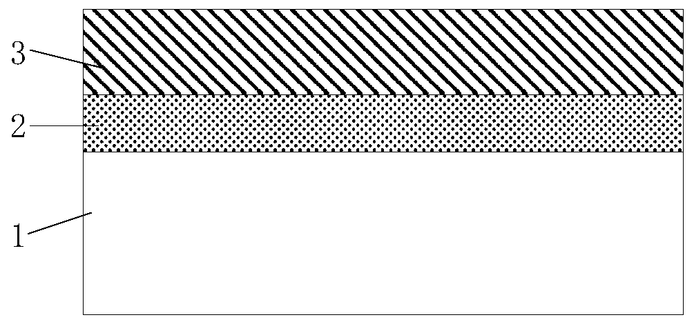
[0029] Such as figure 1 As shown, the present invention is a structure for improving the ohmic contact performance of GaN on the N polar plane, said structure comprising a GaN material, a TiN thin layer ( 2), and a metal stack (3) covering the TiN thin layer (2).

[0030] Preferably, the GaN epitaxial layer (1) is a GaN epitaxial layer (1) with an N polar surface and unintentionally doped, and the thickness of the GaN epitaxial layer (1) is 10nm-500μm

[0031] Preferably, the thickness of the TiN thin layer is 1-100 nm.

[0032] Preferably, the metal in the metal stack (3) is a non-Au metal compatible w...


PUM

PropertyMeasurementUnit
Thicknessaaaaaaaaaa
Thicknessaaaaaaaaaa
Specific contact resistivityaaaaaaaaaa

Abstract

The invention relates to a structure for improving ohmic contact performance of an N-polar surface GaN. The structure comprises a GaN material, a TiN thin layer (2) covering an epitaxial layer (1) ofthe N-polar surface GaN of the GaN material, and a metal laminated layer (3) covering the TiN thin layer (2). The invention has the following beneficial effects that the TiN thin layer has the advantages of high melting point, low work function and the like; the TiN thin layer can form a stable contact interface with the N-polar surface GaN under the condition of high temperature, so that the reaction between the ohmic contact metal and the N-polar surface GaN material is effectively inhibited, and after the ohmic metal layer is annealed in the atmosphere of protective gas, ohmic contact degradation cannot be caused, and better ohmic contact characteristics can be formed. According to the invention, the thermal stability of the ohmic contact of the N-polar surface GaN is improved, and thespecific contact resistivity of the ohmic contact of the N-polar surface GaN is reduced, so that the overall performance of the device is improved. The method is simple in process and high in repeatability and reliability.

Description

technical field [0001] The invention relates to the field of GaN semiconductor device technology, in particular to a method for using TiN with good thermal stability as an N-polar surface GaN ohmic contact electrode to improve its stability. Background technique [0002] Gallium Nitride (GaN), as a third-generation semiconductor material, has become a research hotspot in the semiconductor field in recent years due to its advantages such as large band gap, high electron saturation rate, and large breakdown electric field. GaN lateral devices on the Ga surface have been gradually industrialized, and have great application prospects in high-frequency, high-power power electronic switching devices. The research on N-side GaN devices has not stopped. Using the polarization effect, the N-side AlGaN / GaN heterojunction can form 2DHG, thereby manufacturing p-channel devices, which can be integrated with n-channel devices to form CMOS devices. In addition, because the vertical device...

Claims


Application Information

Patent Timeline
IPC IPC(8): H01L29/45H01L21/28
CPCH01L29/452H01L29/401
Inventor 刘扬丘秋凌李柳暗
Owner SUN YAT SEN UNIV
Why Eureka
Try Eureka