Different-plane structure GaAs photoconductive switch based on graphene interface layer and preparation process thereof

A photoconductive switch, graphene layer technology, applied in sustainable manufacturing/processing, semiconductor devices, final product manufacturing, etc. The effect of suppressing heat accumulation and improving reliability

Active Publication Date: 2020-05-08
XI AN JIAOTONG UNIV
View PDF5 Cites 4 Cited by
  • Summary
  • Abstract
  • Description
  • Claims
  • Application Information

AI Technical Summary

Problems solved by technology

[0004] In order to solve the above problems, the present invention provides a GaAs photoconductive switch with a heteroplane structure based on a graphene interface layer and its preparation process. At present, most photoconductive switches are produced around the principle of forming ohmic contacts between gallium arsenide and multilayer metals. , but the switching device is faced with short life, uneven heat dissipation, and easy burnout. The present invention transfers high-quality graphene to the target substrate and then coats the surface with metal to form a gallium arsenide-graphene-metal Composite structure, homogeneous electric field, current is not concentrated, and relatively less heat is generated, which has a great effect on the heat dissipation and life of the device

Method used


Image

  • Different-plane structure GaAs photoconductive switch based on graphene interface layer and preparation process thereof
  • Different-plane structure GaAs photoconductive switch based on graphene interface layer and preparation process thereof
  • Different-plane structure GaAs photoconductive switch based on graphene interface layer and preparation process thereof

Examples


Embodiment 1

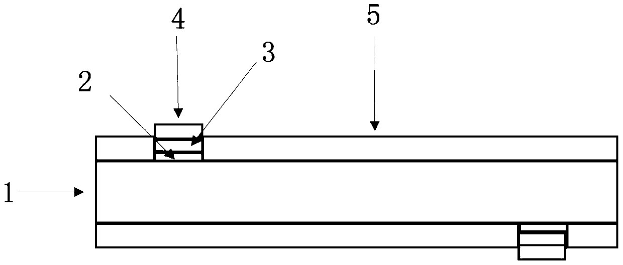
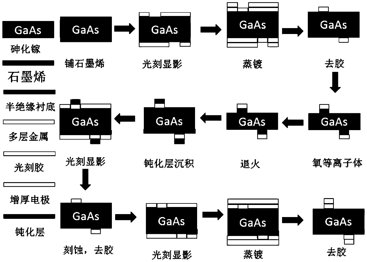
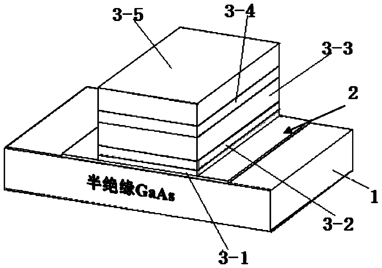
[0087] Select a semi-insulating gallium arsenide double-polished wafer with a crystal orientation , with a thickness of 600 μm, and use acetone, sulfuric acid and other processes to clean the surface of the gallium arsenide to remove surface impurities.

[0088] 1) Preparation of composite structure of CVD graphene and gallium arsenide

[0089] On a Cu foil with a thickness of 25 μm, graphene is grown by CVD, and the graphene is transferred to a semi-insulating GaAs surface by a pulling method to obtain a first composite structure.

[0090] 2) Graphicalize the first composite structure:

[0091] The first photolithography (front and back):

[0092] (1) Coating photoresist AZ-5214 (2) Coating (3) Pre-baking (4) Exposure (5) Development (6) Post-baking (7) UVO to remove residual glue;

[0093] 3) Then make five layers of metal (front and back) on the surface as electrodes (Ni layer, Ge layer, Au layer, Ni layer and Au layer). The total thickness of the five layers of metal is ...

Embodiment 2

[0104] Select a four-inch gallium arsenide double-polished wafer with crystal orientation , resistivity ≥ 10 Ωcm, thickness 600 μm, use acetone, sulfuric acid and other processes to clean the surface of gallium arsenide to remove surface impurities.

[0105] 1) Preparation of composite structure of CVD graphene and gallium arsenide

[0106] On a Cu foil with a thickness of 25 μm, graphene is grown by CVD, and the graphene is transferred to a semi-insulating GaAs surface by a pulling method to obtain a first composite structure.

[0107] 2) Graphicalize the first composite structure:

[0108] The first photolithography (front and back):

[0109] (1) Coating photoresist AZ-5214 (2) Coating (3) Pre-baking (4) Exposure (5) Development (6) Post-baking (7) UVO to remove residual glue;

[0110] 3) Then make five layers of metal (front and back) on the surface as electrodes (Ni layer, Ge layer, Au layer, Ni layer and Au layer). The total thickness of the five layers of metal is 296....

Embodiment 3

[0121] Select a four-inch gallium arsenide double-polished wafer with crystal orientation , resistivity ≥ 10 Ωcm, thickness 600 μm, use acetone, sulfuric acid and other processes to clean the surface of gallium arsenide to remove surface impurities.

[0122] 1) Preparation of composite structure of CVD graphene and gallium arsenide

[0123] On a Cu foil with a thickness of 25 μm, graphene is grown by CVD, and the graphene is transferred to a semi-insulating GaAs surface by a pulling method to obtain a first composite structure.

[0124] 2) Graphicalize the first composite structure:

[0125] The first photolithography (front and back):

[0126] (1) Coating photoresist AZ-5214 (2) Coating (3) Pre-baking (4) Exposure (5) Development (6) Post-baking (7) UVO to remove residual glue;

[0127] 3) Then make five layers of metal (front and back) on the surface as electrodes (Ni layer, Ge layer, Au layer, Ni layer and Au layer). The total thickness of the five layers of metal is 296....


PUM

PropertyMeasurementUnit
thicknessaaaaaaaaaa
thicknessaaaaaaaaaa
thicknessaaaaaaaaaa

Abstract

The invention discloses a different-plane structure GaAs photoconductive switch based on a graphene interface layer and a preparation process of the different-plane structure GaAs photoconductive switch. Contact electrodes are arranged on the upper surface and the lower surface of the GaAs substrate, the two contact electrodes are respectively used as an anode and a cathode of the GaAs photoconductive switch, external electrodes are arranged on the surfaces of the two contact electrodes, graphene layers are arranged between the two contact electrodes and the GaAs substrate, the upper surface of the GaAs substrate is further covered with a passivation layer, and the contact electrodes are sequentially provided with a Ni layer, a Ge layer, an Au layer, a Ni layer and an Au layer in the direction from the graphene layers to the external electrodes. High-quality graphene is transferred to the target substrate, and then the surface of the target substrate is plated with metal to form a gallium arsenide-graphene-metal composite structure, so that an electric field is homogenized, current is not concentrated, generated heat is relatively less, and the method plays a great role in heat dissipation and service life of a device.

Description

technical field [0001] The invention relates to the technical field of a gallium arsenide photoconductive switch, in particular to a GaAs photoconductive switch with a heteroplane structure based on a graphene interface layer and a preparation process thereof. Background technique [0002] Gallium arsenide photoconductive switch has many advantages, such as simple structure, fast response speed, high voltage resistance, small trigger jitter, high switching precision, and can be used for high switching precision, THz technology, high-power optical communication and high-noise environment. Electronics and transient electromagnetic wave technology have broad application prospects, and they also have important applications in fields such as weapon ignition, radar communication, and environmental monitoring, and photoconductive switches are gradually showing important applications in other fields such as biology and medicine. [0003] However, traditional gallium arsenide photoco...

Claims


Application Information

Patent Timeline
Patent Type & Authority Applications(China)
IPC IPC(8): H01L31/024H01L31/0224H01L31/09H01L31/18
CPCH01L31/024H01L31/0224H01L31/09H01L31/184Y02P70/50
Inventor 胡龙李昕崔宏旺朱莉刘康孙岳
Owner XI AN JIAOTONG UNIV
Why Eureka
Try Eureka