Monocrystalline silicon wafer with pyramid superposition structure and preparation method

A single crystal silicon wafer and pyramid technology, which is applied in the field of solar cells, can solve the problems of insufficient contact between the small pyramid suede and the conductive grid lines, increase the contact resistance, and reduce the welding tension of the grid lines, so as to achieve good welding reliability, The effect of high short-circuit current and low reflectivity

Inactive Publication Date: 2020-05-19
ZHONGWEI NEW ENERGY CHENGDU CO LTD
View PDF4 Cites 6 Cited by
  • Summary
  • Abstract
  • Description
  • Claims
  • Application Information

AI Technical Summary

Problems solved by technology

However, silicon wafers with small pyramid sizes have other problems. For example, when screen-printing conductive grid lines, the contact between the small pyramid suede and the conductive grid lines is insufficient, which increases the contact resistance and reduces the welding tension of the grid lines.

Method used


Image

  • Monocrystalline silicon wafer with pyramid superposition structure and preparation method
  • Monocrystalline silicon wafer with pyramid superposition structure and preparation method
  • Monocrystalline silicon wafer with pyramid superposition structure and preparation method

Examples


Embodiment 1

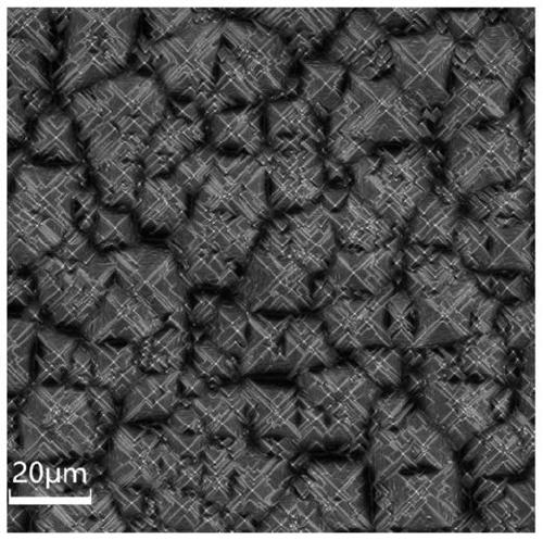
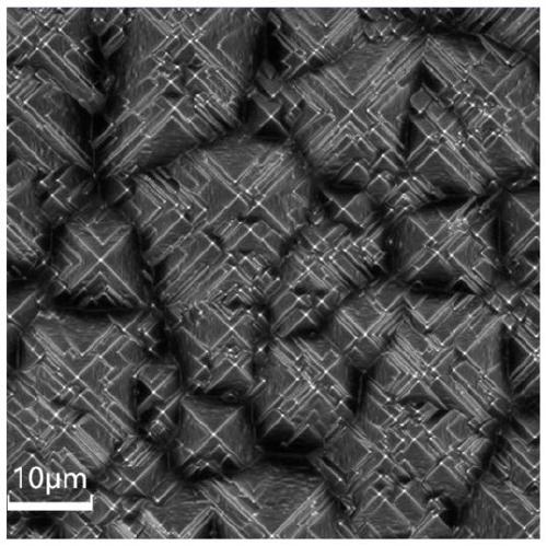
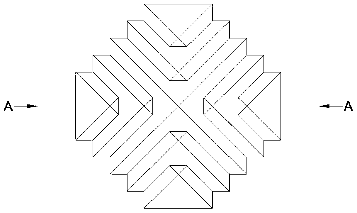
[0029] refer to Figure 1~6 , a single crystal silicon wafer with a pyramid superposition structure, including a silicon wafer whose surface is covered with pyramid units after textured.

[0030] As a preferred manner, the pyramid unit includes a large pyramid, and the surface of the large pyramid is sequentially stacked with small pyramids from top to bottom.

[0031] As a preferred manner, the length of the base of the small pyramid is less than half of that of the large pyramid.

[0032] As a preferred manner, the bottom area of ​​the pyramid units is 1-500 square microns.

[0033] As a preferred manner, the number of pyramids included in the pyramid unit is 5-500.

[0034] The above-mentioned method for preparing a single crystal silicon wafer with a pyramid superposition structure is characterized in that it comprises the following steps:

[0035] A. Pre-cleaning to remove the surface contamination of the original silicon wafer. Use one or more of ammonia water, sodiu...

Embodiment 2

[0044] refer to Figure 1~6 , in this embodiment, optional but not limited to using the texture additive of Nippon Hayashi pure HPC to prepare the texture of the pyramid superposition structure, the specific steps are as follows:

[0045] (1) Pre-cleaning

[0046] Clean the original silicon chip in a mixed solution of ammonia water and hydrogen peroxide, the mass concentration of ammonia water in the solution is 3%, the mass concentration of hydrogen peroxide is 3%, the temperature is 65° C., and the cleaning time is 5 minutes. After cleaning, rinse the silicon wafer in pure water at room temperature for 3 minutes.

[0047] (2) The first step of cashmere

[0048] Use Nippon Hayashi pure HPC texture additive, the mass concentration of each component in the solution: potassium hydroxide is 7.5%, TK81 is 4%, TT72C13 is 0.6%, the temperature is 85°C, and the time is 15min. Rinse the silicon wafer in pure water at room temperature for 3 minutes after texturing.

[0049] (3) The...

Embodiment 3

[0066] refer to Figure 1~6 , in this embodiment, optional but not limited to using the texture additive of ICB of Germany to prepare the texture of the pyramid superposition structure, the specific steps are as follows:

[0067] (1) Pre-cleaning

[0068] Clean the original silicon chip in a mixed solution of potassium hydroxide and hydrogen peroxide, the mass concentration of potassium hydroxide in the solution is 1.5%, the mass concentration of hydrogen peroxide is 3%, the temperature is 65° C., and the cleaning time is 5 minutes. After cleaning, rinse the silicon wafer in pure water at room temperature for 3 minutes.

[0069] (2) The first step of cashmere

[0070] Use the German ICB texturing additive, the mass concentration of each component in the solution: potassium hydroxide is 4.5%, ICBUltra M is 0.8%, the temperature is 85°C, and the time is 10min. Rinse the silicon wafer in pure water at room temperature for 3 minutes after texturing.

[0071] (3) The second ste...


PUM


Abstract

The invention relates to the field of solar cells and discloses a monocrystalline silicon wafer with a pyramid superposition structure and a preparation method. After an original silicon wafer is cleaned through a solution a, anisotropic corrosion is carried out through a solution b to obtain a large pyramid textured surface, and then, secondary texturing is carried out through a solution c, so that a small pyramid textured surface with a smaller size is formed on the original large pyramid textured surface, small pyramids are sequentially stacked on the surface of the large pyramid from top to bottom to form pyramid units; since the pyramid units cover the surface of the silicon wafer and are superposed, the monocrystalline silicon wafer not only has the advantages of good contact betweenthe large pyramid and the conductive grid line and high welding tension, but also has the advantages of low reflectivity of the small pyramid and high short-circuit current. The textured surface of the monocrystalline silicon wafer is of a pyramid superposition structure with different sizes, so that the monocrystalline silicon wafer not only has the advantages of good contact between the large pyramid and the conductive grid line and high welding tension, but also has the advantages of low reflectivity of the small pyramid and high short-circuit current.

Description

technical field [0001] The invention relates to the field of solar cells, in particular to a monocrystalline silicon wafer with a pyramid superposition structure and a preparation method thereof. Background technique [0002] In the manufacturing process of monocrystalline silicon solar cells, a pyramid-shaped light-trapping structure can be formed on the surface of the silicon wafer through wet grooving, and sunlight is reflected twice on the surface of the pyramid, thereby increasing the light absorption rate of the silicon wafer. Improve the current density and photoelectric conversion efficiency of solar cells. This light-trapping suede surface is formed by anisotropic corrosion of silicon wafers in alkaline solution. The crystal plane index on the surface of silicon wafers is (100), and anisotropy occurs in alkaline solutions containing texturing additives. During the chemical reaction, the surface with crystal plane index (100) gradually disappears, and a pyramid morp...

Claims


Application Information

Patent Timeline
IPC IPC(8): H01L31/0236H01L31/18
CPCH01L31/02363H01L31/1804Y02E10/547Y02P70/50
Inventor 杜俊霖韩安军孙林付昊鑫
Owner ZHONGWEI NEW ENERGY CHENGDU CO LTD
Why Eureka
Try Eureka