
Back electric field structure of MWT solar cell and manufacturing method of back electric field structure

A technology for a solar cell and a manufacturing method, applied in the field of solar cells, can solve problems such as reducing area, and achieve the effect of reducing area, reducing consumption, safe and efficient continuous operation

Pending Publication Date: 2020-05-29
HENGDIAN GRP DMEGC MAGNETICS CO LTD
View PDF7 Cites 1 Cited by
  • Summary
  • Abstract
  • Description
  • Claims
  • Application Information

AI Technical Summary

Problems solved by technology

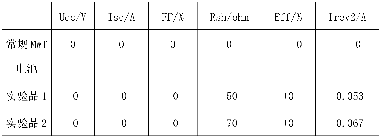
[0005] The present invention mainly solves the original technical problems that Al metal consumption is large and through-hole electrodes are affected by Al metal, and provides a back electric field structure and manufacturing method of MWT solar cells, creating an all-aluminum back field and aluminum grid on the back of MWT cells. The design of the combination of wires reduces the consumption of Al metal paste without affecting the conversion efficiency, and the all-aluminum back field is designed as an aluminum grid line outside the isolation groove in the through-hole electrode area on the back of the battery, which reduces the number of through-hole electrodes. The area of ​​the Al back field outside the regional isolation groove greatly prevents Al metal powder residue from affecting the through-hole electrodes, ensuring the safe and efficient continuous operation of MWT solar cells

Method used


Image

  • Back electric field structure of MWT solar cell and manufacturing method of back electric field structure
  • Back electric field structure of MWT solar cell and manufacturing method of back electric field structure
  • Back electric field structure of MWT solar cell and manufacturing method of back electric field structure

Examples


Embodiment

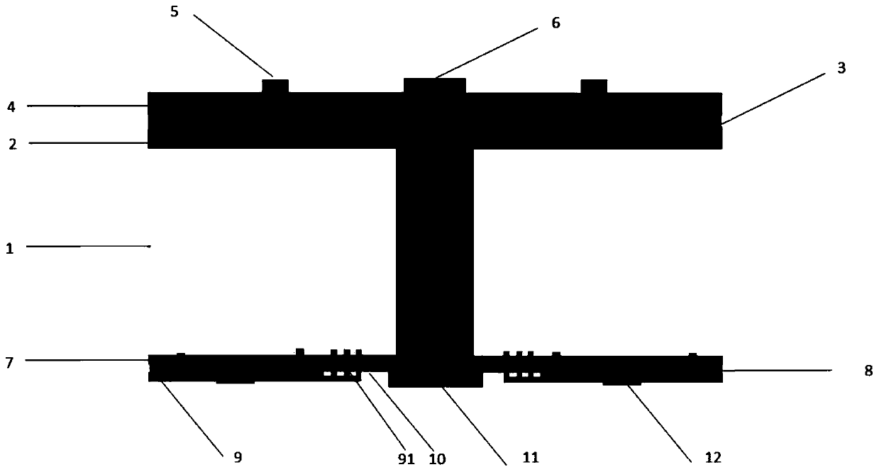
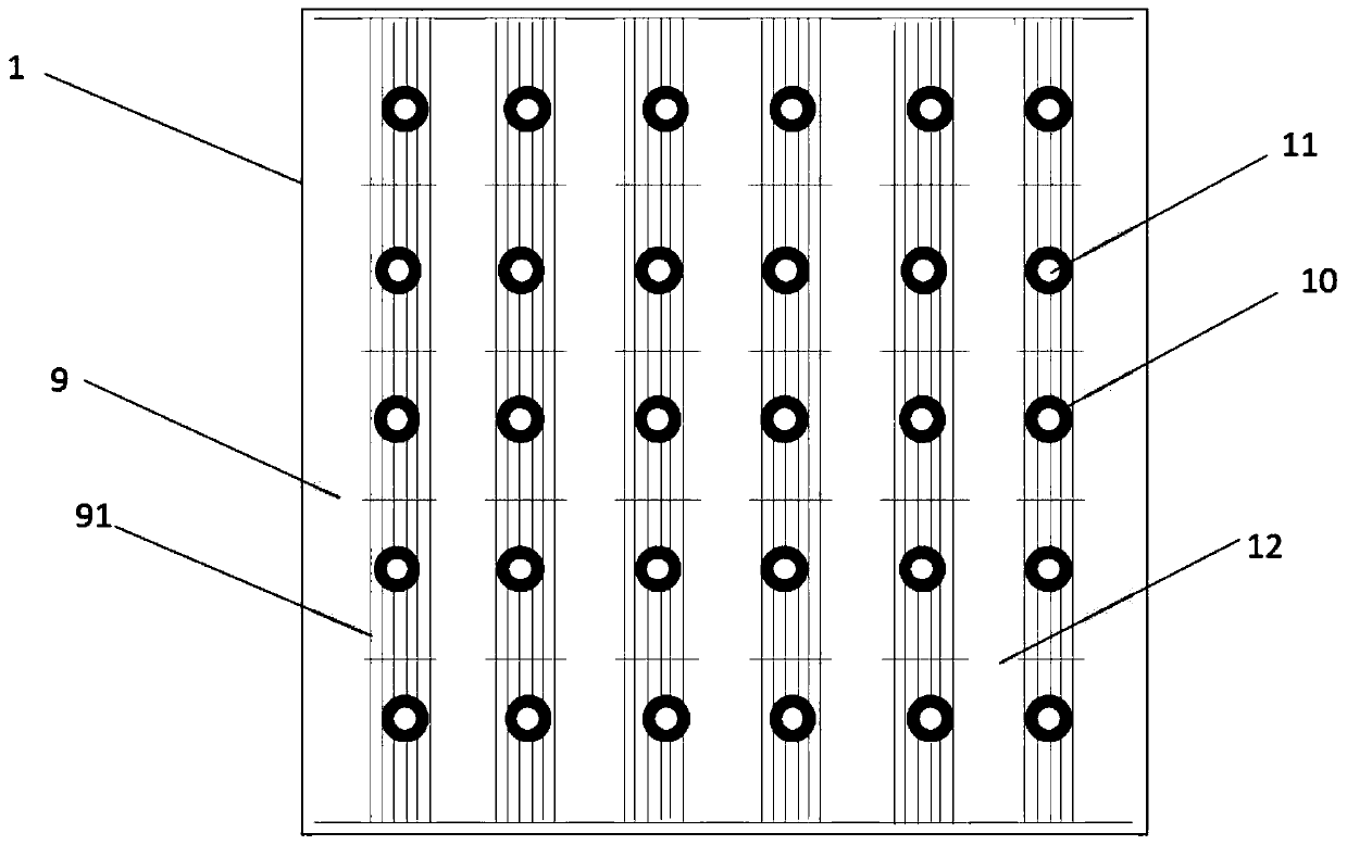
[0031] Embodiment: a kind of MWT solar cell back field structure of this embodiment, such as figure 1 and figure 2As shown, it includes a front silicon nitride film 4, a silicon dioxide film 3, a PN junction 2, a silicon wafer 1, an aluminum oxide film 7 and a back silicon nitride film 8 stacked sequentially from top to bottom. The positive electrode silver grid line 5 and the front side of the through-hole electrode 6 are provided, the back side is provided with an all-aluminum back field 9, the back side of the through-hole electrode 11 and evenly distributed back electrodes 12, and the all-aluminum back field 9 is provided with an aluminum grid line back field 91 , a through-hole isolation groove 10 is provided between the aluminum gate line back field 91 and the back through-hole electrode 11 . The part of the back field outside the isolation groove 10 in the through-hole electrode area on the back of the battery is designed from the all-aluminum back field 9 to the alum...


PUM

PropertyMeasurementUnit
Diameteraaaaaaaaaa
Thicknessaaaaaaaaaa
Thicknessaaaaaaaaaa

Abstract

The invention discloses a back electric field structure of an MWT solar cell. The back electric field structure comprises a front silicon nitride film, a silicon dioxide film, a PN junction, a siliconwafer, an aluminum oxide film and a back silicon nitride film which are all sequentially stacked from top to bottom; the front surface of the silicon wafer is provided with positive electrode silvergrid lines and a through hole electrode front surface; the back surface of the silicon wafer is provided with an all-aluminum back surface field, a through hole electrode back surface and uniformly-distributed back electrodes; the all-aluminum back surface field is provided with aluminum grid line back surface fields; through hole isolation grooves are arranged between the aluminum grid line backsurface fields and a back surface through hole electrode. The invention discloses a manufacturing method of the back electric field of the MWT solar cell. The manufacturing method comprises the following steps of: laser drilling; texturing; diffusion; mask printing; etching; annealing; film coating ; back surface laser grooving; screen printing; and sintering. The design mode of combining the all-aluminum back surface field and the aluminum grid lines is realized on the back surface of the MWT cell in ingeniously; the consumption of Al metal slurry is reduced while conversion efficiency not influenced; the influence of Al metal powder residues on the through hole electrode is greatly avoided; and the safe, efficient and continuous operation of the MWT solar cell is ensured.

Description

technical field [0001] The invention relates to the technical field of solar cells, in particular to a back electric field structure of a MWT solar cell and a manufacturing method thereof. Background technique [0002] According to data, it is a technical challenge that the photovoltaic industry has been facing to achieve higher conversion efficiency of crystalline silicon solar cells while reducing production costs. According to the basic structure and working process analysis of crystalline silicon solar cells, the technical factors affecting the conversion efficiency of crystalline silicon solar cells include three aspects: 1. Optical loss in the absorption process, referred to as optical loss; 2. Photoexcited electron space in the photoconversion process The recombination of hole pairs is referred to as recombination loss; 3. The loss in the current output process is referred to as electrical loss. The influencing factors of the optical loss include the shallow surface ...

Claims


Application Information

Patent Timeline
IPC IPC(8): H01L31/0224
CPCH01L31/02245Y02E10/50Y02P70/50
Inventor 黎剑骑孙涌涛许成德王富强楼诚侃
Owner HENGDIAN GRP DMEGC MAGNETICS CO LTD
Learn More