Novel electron transport layer perovskite solar cell and preparation method thereof

A technology of electron transport layer and solar cell, which is applied in circuits, photovoltaic power generation, electrical components, etc., can solve the problems of high defect density, poor stability, and low electron mobility of the electron transport layer, so as to reduce the recombination rate and improve stability , Improve the effect of photoelectric conversion efficiency

Active Publication Date: 2020-06-09
QILU UNIV OF TECH
View PDF6 Cites 3 Cited by
  • Summary
  • Abstract
  • Description
  • Claims
  • Application Information

AI Technical Summary

Problems solved by technology

[0004] The object of the present invention is to provide a novel electron transport layer perovskite solar cell and its preparation method to solve the problems of low electron mobility, poor stability, and high defect density in the existing perovskite solar cell electron transport layer, and to obtain high Stable, high energy conversion efficiency perovskite solar cells

Method used


Image

  • Novel electron transport layer perovskite solar cell and preparation method thereof

Examples


Embodiment 1

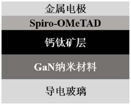
[0030] A novel GaN electron transport layer perovskite solar cell and a preparation method thereof, the preparation method comprising the following steps:

[0031] (1) After cleaning the fluorine-doped tin oxide (FTO) conductive glass, process it with a plasma cleaning machine to obtain a pretreated conductive glass substrate at last;

[0032] (2) Put GaN powder with a particle size of 100 μm, deionized water and ball milling medium into the ball mill tank at a ratio of 20:1:1, use a high-energy ball mill to mill at an ultra-high speed of 800 r / min for 25 hours, take it out and put it in 80 Dry in an oven at ℃ to obtain GaN nanomaterials with a particle size of 100nm, disperse the GaN materials in absolute ethanol at a mass ratio of 0.2, and ultrasonicate for 1h to obtain a GaN dispersion; spin-coat the GaN dispersion on an FTO conductive glass substrate, The spin coating speed is 4000r / min, and then transferred to a heating table with a temperature of 150°C, and kept for 30mi...

Embodiment 2

[0037] (1) After cleaning the indium tin oxide (ITO) conductive glass, process it with a plasma cleaning machine, and finally obtain a pretreated conductive glass substrate;

[0038] (2) Put GaN powder with a particle size of 150 μm, deionized water and ball milling medium into the ball milling tank at a ratio of 30:1:1, use a high-energy ball mill to mill at an ultra-high speed of 1100r / min for 30 hours, take it out and put it in 80 Dry in an oven at ℃ to obtain GaN nanomaterials with a particle size of 110 nm. GaN materials are dispersed in absolute ethanol at a mass ratio of 0.25, and ultrasonicated for 2 hours to obtain a GaN dispersion. Spin-coat the GaN dispersion on the ITO conductive glass substrate at a spin-coating speed of 5000r / min, then transfer to a heating table at a temperature of 200°C and keep it warm for 40min to prepare the GaN electron transport layer;

[0039] (3) The spin coating component on the prepared GaN electron transport layer is FA 0.83 MA 0.17...


PUM

PropertyMeasurementUnit
particle diameteraaaaaaaaaa
thicknessaaaaaaaaaa

Abstract

The invention belongs to the technical field of semiconductor devices, and particularly relates to a novel electron transport layer perovskite solar cell and a preparation method thereof. The method comprises the steps of (1) cleaning conductive glass, and processing the cleaned conductive glass through a plasma cleaning machine to obtain a pretreated conductive glass substrate; (2) preparing a GaN nano material by adopting a high-energy ball milling method, then spin-coating GaN dispersion liquid on the conductive glass substrate, and transferring to a heating table to prepare a GaN electrontransport layer; (3) spin-coating a perovskite precursor solution on the GaN electron transport layer, and rapidly transferring the GaN electron transport layer to a preheated heating table after spin-coating is finished to prepare a perovskite layer; (4) spin-coating a hole transport layer on a perovskite light absorption layer; and (5) evaporating an electrode on the prepared hole transport layer to complete the preparation of the perovskite solar cell. The GaN nano material is used as the electron transport layer, the electron transport efficiency of the solar cell can be improved, and therecombination rate is reduced, so that the photoelectric conversion efficiency and stability of the device are remarkably improved.

Description

technical field [0001] The invention belongs to the technical field of semiconductor devices, and in particular relates to a novel electron transport layer perovskite solar cell and a preparation method thereof. Background technique [0002] Solar energy is considered as a clean, safe, inexhaustible and ideal renewable energy, and is receiving more and more attention. In this context, the development of new high-efficiency and low-cost solar cells has aroused great interest of researchers from all over the world. Perovskite solar cells have rapidly become a global research hotspot since they were first proposed in 2009, and their advantages of low cost, solution processability and excellent photoelectric conversion performance have attracted much attention internationally. [0003] Perovskite solar cells generally consist of a conductive glass substrate, an electron transport layer, a perovskite light absorbing layer, a hole transport layer, and metal electrodes. Among the...

Claims


Application Information

Patent Timeline
Patent Type & Authority Applications(China)
IPC IPC(8): H01L51/42H01L51/48
CPCH10K71/12H10K30/15Y02E10/549
Inventor 俞娇仙张雷刘光霞王泰林陈成敏
Owner QILU UNIV OF TECH
Why Eureka
Try Eureka