Unlock instant, AI-driven research and patent intelligence for your innovation.
Method for preparing grating with submicron structure
What is Al technical title?
Al technical title is built by PatSnap Al team. It summarizes the technical point description of the patent document.
A sub-micron and grating technology, which is applied in the field of preparation of sub-micron structured gratings, to achieve the effects of improving diffraction efficiency, good grating uniformity, and high pattern accuracy
Inactive Publication Date: 2020-06-19
HUAZHONG UNIV OF SCI & TECH
View PDF8 Cites 3 Cited by
Summary
Abstract
Description
Claims
Application Information
AI Technical Summary
This helps you quickly interpret patents by identifying the three key elements:
Problems solved by technology
Method used
Benefits of technology
Problems solved by technology
The difficulty lies in the control of the imprinting parameters, and finally the dry etching of the substrate determines the quality of the grating
Method used
Image
Click on the blue label to locate the original text in one second.
Reading with bidirectional positioning of images and text.
Examples
preparation example Construction
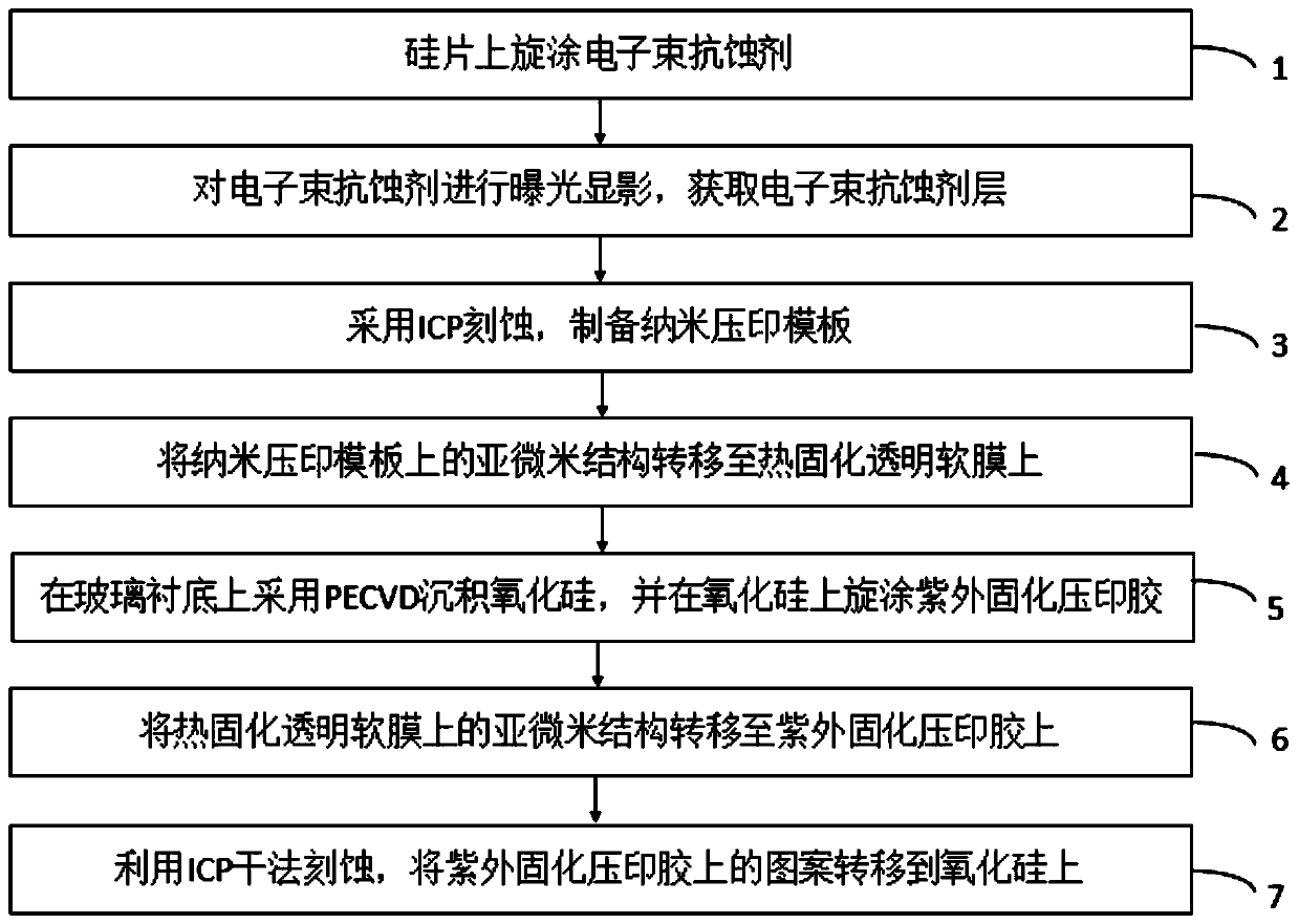
[0037] The present invention provides a method for preparing a submicron structure grating, which includes the following steps:
[0039] Among them, the beam current of electron beam exposure is 1nA~20nA; the dose of electron beam exposure is 100μC / cm 2 ~300μC / cm 2 ;
[0040] (2) Use the electron beam resist layer as a mask to perform dry etching to prepare a nanoimprint template;
[0041] Among them, the dry etching gas in step (2) includes SF 6 And C 4 F 8 ;SF 6 The air flow is 4sccm~20sccm; C 4 F 8 The gas flow rate is 4sccm~20sccm; the cavity pressure of dry etching is 4mTorr~25mTorr; the radio frequency power is: 10W-50W; the inductive coupling power is 100W~1500W;
[0042] (3) Transfer the sub-micron structure on the nanoimprint template to the thermally cured transparent soft film, and spin-coat the UV-curable imprint glue on the subs...
Embodiment
[0055] Such as figure 1 As shown, this embodiment provides a method for preparing a sub-micron structure grating, including the following steps:
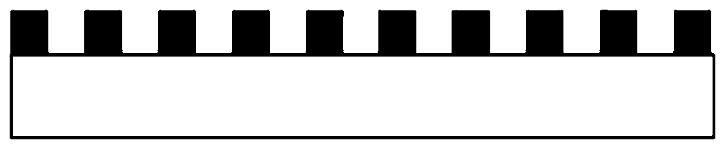
[0056] Step 1: Take a 430 micron thick 2-inch p-type For silicon wafers with crystal orientation, after conventional wet cleaning, the electron beam resist ARP6200.09 is spin-coated on the silicon wafer, see Figure 2(a) to obtain the electron beam resist;
[0057] Step 2: Perform electron beam exposure on the electron beam resist, the exposure dose is 240μC / cm 2 , The current is 15nA; after the exposure is completed, develop with MIBK for 40s and fix with isopropanol for 70s. See Figure 2(b) to obtain the electron beam resist layer;
[0058] Step 3: Use the electron beam resist layer exposed by the electron beam as the mask of the silicon wafer, and use ICP etching to prepare the nanoimprint template, see Figure 2(c);
[0059] Among them, the etching parameters are: SF 6 The flow rate is 12sccm; C 4 F 8 The flow rate is 12sccm; the radio fr...
PUM
Abstract
The invention discloses a method for preparing a grating with a submicron structure, which belongs to the technical field of microstructures in semiconductors, and particularly comprises the followingsteps of: spin-coating an electron beam resist on a siliconwafer, and performing electron beam exposure to obtain an electron beam resist layer; performing dry etching by taking the electron beam resist layer as a mask to prepare a nanoimprint template; transferring the submicron structure on the nanoimprint template to a thermocuring transparent soft film; spin-coating an ultraviolet curing imprinting adhesive on the substrate for preparing the grating; transferring the submicron structure on the thermocuring transparent soft film to an ultraviolet curing imprinting adhesive through a nanoimprinting method; and transferring the submicron pattern on the ultraviolet curing impressing adhesive to a substrate for preparing the grating by using a dry etching method. The nanoimprint templateprepared through electron beam exposure and dry etching is high in pattern precision and smooth in surface. The sub-micron structure grating prepared through soft film transfer printing, nanoimprint lithography and dry etching is good in uniformity, high in yield, accurate in size and low in cost.
Description
Technical field [0001] The invention belongs to the technical field of microstructures in semiconductor science, and more specifically relates to a method for preparing a submicron structure grating. Background technique [0002] With the development and progress of semiconductor technology, the scale of microstructures has reached nano-processing precision. Among them, laserdirect writing, ultraviolet lithography, electron beam exposure and nanoimprinting can all make sub-micron gratings. However, large-area fabrication of submicron structures still has problems such as high cost and difficulty in fabrication. At present, high-precision sub-micron grating imprint templates are generally produced by a combination of electron beam exposure and dry etching. Among them, the difficulty of electron beam exposure lies in the control of exposure parameters and how to prevent overexposure or underexposure. The problem of defects in graphics; the dry etching parameters of the grating im...
Claims
Application Information
Patent Timeline
Application Date:The date an application was filed.
Publication Date:The date a patent or application was officially published.
First Publication Date:The earliest publication date of a patent with the same application number.
Issue Date:Publication date of the patent grant document.
PCT Entry Date:The Entry date of PCT National Phase.
Estimated Expiry Date:The statutory expiry date of a patent right according to the Patent Law, and it is the longest term of protection that the patent right can achieve without the termination of the patent right due to other reasons(Term extension factor has been taken into account ).
Invalid Date:Actual expiry date is based on effective date or publication date of legal transaction data of invalid patent.

