Silicon carbide diode with low turn-on voltage and low on resistance and manufacturing method

A technology of silicon carbide diodes and low on-resistance, applied in semiconductor/solid-state device manufacturing, circuits, electrical components, etc., can solve problems such as large reverse leakage current, high turn-on voltage, and small forward turn-on voltage The effect of high withstand voltage, small on-resistance, and low turn-on voltage

Active Publication Date: 2020-06-19
UNIV OF ELECTRONICS SCI & TECH OF CHINA
View PDF11 Cites 18 Cited by
  • Summary
  • Abstract
  • Description
  • Claims
  • Application Information

AI Technical Summary

Problems solved by technology

PiN diodes have the advantages of high withstand voltage and low reverse leakage current, but the built-in potential of PiN diodes is relatively high, and the turn-on voltage is high; in addition, as a bipolar device, the conductance modulation effect produces a large number of minority loads in the drift region. The current greatly improves the conduction capability of the device and reduces the conduction loss; on the contrary, it also reduces the turn-off speed of the device, which limits the development of the diode to high frequency
Schottky diodes have a small forward turn-on voltage. As a unipolar device, there is no minority carrier storage effect, and the switching speed is fast, but the reverse leakage current is large, so it is difficult to apply to high-voltage and high-current fields.
[0004] In order to solve the problems of high turn-on voltage of traditional diodes and large leakage current of Schottky diodes, the present invention proposes a silicon carbide diode structure with three accumulation channels, low turn-on voltage and low on-resistance

Method used


Image

  • Silicon carbide diode with low turn-on voltage and low on resistance and manufacturing method
  • Silicon carbide diode with low turn-on voltage and low on resistance and manufacturing method
  • Silicon carbide diode with low turn-on voltage and low on resistance and manufacturing method

Examples


Embodiment Construction

[0036] The following describes the embodiments of the present invention, and those skilled in the art can easily understand other advantages and effects of the present invention from the content disclosed in this specification. The present invention can also be implemented or applied through other different specific embodiments, and various details in this specification can also be modified or changed based on different viewpoints and applications without departing from the spirit of the present invention.

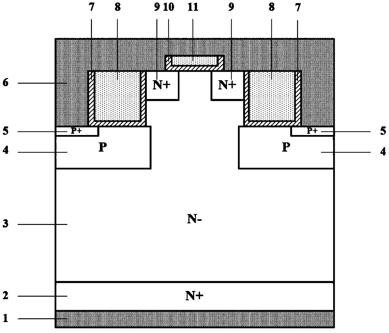
[0037] A silicon carbide diode with low turn-on voltage and low on-resistance, comprising a cathode metal electrode 1, an N+ substrate above the cathode metal electrode 1, an N-drift region 3 above the N+ substrate 2, and an N-drift region 3 The upper P-type shielding buried layer 4, the P+ ohmic contact area 5 located inside the P-type shielding buried layer 4, the anode metal electrode 6 located above the P+ ohmic contact area 5, and the trench gate dielectric layer above th...


PUM


Abstract

The invention provides a silicon carbide diode with low turn-on voltage and low on resistance and a manufacturing method thereof. The silicon carbide diode comprises a cathode metal electrode, an N +substrate above the cathode metal electrode and an N-drift region above the N + substrate, a P-type shielding buried layer arranged above the N-drift region; a P + ohmic contact region arranged in theP-type shielding buried layer, an anode metal electrode arranged above the P + ohmic contact region, a trench gate dielectric layer arranged above the P-type shielding buried layer, a polysilicon trench gate arranged in the trench gate dielectric layer, an N+ source regions arranged between the trench gate dielectric layers, a plane gate dielectric layer arranged above the N + source regions, anda polysilicon plane gate arranged in the plane gate dielectric layer. The anode metal electrode covers the trench gate dielectric layer, the polysilicon trench gate, the N+ source region, the plane gate dielectric layer and the polysilicon plane gate. According to the invention, the three-channel accumulation type channel MOSFET and the JFET are connected in series to form the super-barrier diode, and the silicon carbide diode has the characteristics of low turn-on voltage, small on-resistance, high reverse withstand voltage, small leakage current and the like.

Description

Technical field [0001] The invention belongs to the technical field of power semiconductors, in particular to a silicon carbide diode with low turn-on voltage and low on-resistance. Background technique [0002] Silicon Carbide is one of the representatives of the third-generation wide-bandgap semiconductor materials. It has the characteristics of large forbidden band width, high critical breakdown electric field, high thermal conductivity and high saturation drift speed of electrons. , High-temperature and high-frequency power electronics have broad application prospects. [0003] Diodes are the earliest electronic devices used. With the innovation of electronic devices, PiN power diodes and Schottky power diodes are the most widely used in high-frequency and high-voltage applications. PiN diode has the advantages of high withstand voltage, low reverse leakage current, etc., but the built-in potential of PiN diode is relatively high, and the turn-on voltage is high; in addition, ...

Claims


Application Information

Patent Timeline
Patent Type & Authority Applications(China)
IPC IPC(8): H01L29/06H01L29/10H01L29/861H01L27/06H01L21/329
CPCH01L29/8613H01L29/6606H01L27/0617H01L29/1025H01L29/0684H01L29/0638H01L29/0623
Inventor 邓小川路晓飞徐晓杰李旭李轩孙燕张波
Owner UNIV OF ELECTRONICS SCI & TECH OF CHINA
Why Eureka
Try Eureka