
Current ripple compensation circuit and method adopting wide bandgap device and silicon-based device

A technology of current ripple and compensation circuit, applied in the field of power electronics, can solve the problems of large switching loss and high price of wide bandgap devices

Active Publication Date: 2020-07-03
HANGZHOU DIANZI UNIV
View PDF4 Cites 4 Cited by
  • Summary
  • Abstract
  • Description
  • Claims
  • Application Information

AI Technical Summary

Problems solved by technology

[0007] In order to solve the problems that the switching loss of the DCDC power converter in the related art is relatively large and the wide bandgap device is not widely used due to the high price of the wide bandgap device and the power device contains the switching ripple component

Method used


Image

  • Current ripple compensation circuit and method adopting wide bandgap device and silicon-based device
  • Current ripple compensation circuit and method adopting wide bandgap device and silicon-based device
  • Current ripple compensation circuit and method adopting wide bandgap device and silicon-based device

Examples


Embodiment 1

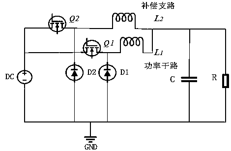
[0067] Such as Figure 1 As shown, the working circuit of a non-isolated ripple-compensated Buck power converter provided in this embodiment includes a parallel power main circuit and a compensation branch, and the DCDC output terminal is connected to a parallel capacitor C through the power main circuit and the compensation branch. Connect to resistor R and connect to ground through capacitor C and resistor R. The main power circuit includes the switch tube IGBT Q in series 1 and power inductor L 1 , switching tube IGBT Q 1 and power inductor L 1 common terminal through the first diode D 1 grounded. The compensation branch includes a series switch GaN device Q 2 and compensation inductance L 2 , switch tube GaN device Q 2 and compensation inductance L 2 common terminal through the second diode D 2 grounded. The power main circuit controls the large current, and the compensation branch is used to compensate the current ripple brought by the power main circuit.

Embodiment 2

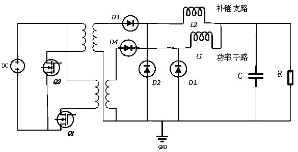
[0069] Such as figure 2 As shown, the working circuit of an isolated forward converter with isolated ripple compensation provided in this embodiment includes a parallel power main circuit and a compensation branch circuit, and the power main circuit includes a switching tube IGBT Q 1 , the fourth diode D 4 and the first diode D 1 , switching tube IGBT Q 1 It is connected in parallel with the power supply DC, and the switching tube IGBT Q 1 with the fourth diode D 4 are isolated by a transformer, the fourth diode D 4 Respectively with the power inductor L 1 and the first diode D 1 connect. The compensation branch includes the switching tube GaN device Q 2 , the third diode D 3 and the second diode D 2 , switch tube GaN device Q 2 It is connected in parallel with the power supply DC, and the switching tube GaN device Q 2 with the third diode D 3 are isolated by a transformer, the third diode D 3 respectively with compensation inductance L 2 and the second diode D...

Embodiment 1

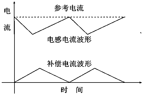
[0071] In Embodiment 1 and Embodiment 2, the main power circuit operates at a low frequency state, flows a large current, and is the main power output circuit. The compensation branch controls the inductance L through the hysteresis 2 The output current is used to track the deviation current between the current reference value and the power main circuit inductor current value, which is used to compensate the current ripple. Finally, the superposition of the two branch currents is equal to the given reference current value, such as image 3 shown. As a result, the output current ripple is greatly reduced, thereby reducing the output voltage ripple.

[0072] A DCDC current ripple active compensation method includes a parallel power main circuit and a compensation branch circuit. The power main circuit operates in a low-frequency state and flows through a large current, and is a main power output circuit. The compensation branch uses hysteresis control to compensate the output...


PUM


Abstract

The invention discloses a current ripple compensation circuit and method adopting a wide bandgap device and a silicon-based device, and belongs to the technical field of power electronics. The methodcomprises the following steps: a silicon-based device is taken as a power main circuit of a switching tube to realize high-power conversion; a wide bandgap device is used as a compensation branch of the switching tube to realize current ripple compensation; the high-power converter main circuit works in a low-frequency state; the current ripple compensation branch works in a high-frequency state;the power main circuit and the compensation branch circuit are connected in parallel. And the high-frequency compensation branch compensates the current ripple of the low-frequency main circuit, and the error between the voltage feedback value and the reference value passes through the voltage controller Gvc to obtain a reference current value Iref. The compensation circuit achieves the compensation of the high-frequency branch for the current ripples of the low-frequency branch while giving play to the advantages of a silicon-based device and a wide bandgap device, and reduces the total costand the conduction loss of a switching tube.

Description

technical field [0001] The invention relates to the technical field of power electronics, in particular to a current ripple compensation circuit and method using wide bandgap devices and silicon-based devices. Background technique [0002] With the continuous development of power electronics towards high frequency and high power, silicon-based semiconductor devices have reached the theoretical limit of the material's own characteristics. The performance of traditional silicon-based devices cannot meet the needs of the power electronics industry, which seriously limits the power electronics industry. industry development. The third-generation wide-bandgap semiconductors represented by silicon carbide (SiC) and gallium nitride (GaN) made breakthroughs in the manufacturing process in the 1990s, and the manufacturing technology has become more mature so far. Today, the third-generation wide-bandgap semiconductors represented by silicon carbide and gallium nitride have become th...

Claims


Application Information

Patent Timeline
IPC IPC(8): H02M1/14H02M1/15
CPCH02M1/143H02M1/15H02M1/0054Y02B70/10
Inventor 沈磊傅伟伟
Owner HANGZHOU DIANZI UNIV
Learn More