
Graphite crucible device for silicon carbide crystal growth and single crystal growth method thereof

A technology of graphite crucible and crystal growth, which is applied in the direction of single crystal growth, crystal growth, single crystal growth, etc. It can solve the problems of increasing wafer cost and increasing annealing process, and achieves the effect of reducing temperature gradient and low stress

Inactive Publication Date: 2020-07-14
NANTONG UNIVERSITY
View PDF4 Cites 7 Cited by
  • Summary
  • Abstract
  • Description
  • Claims
  • Application Information

AI Technical Summary

Problems solved by technology

However, this annealing treatment does not necessarily completely eliminate the internal stress in the wafer
Because there is also a temperature gradient in the annealing furnace, it cannot be completely avoided
Moreover, the annealing needs to be continued for a long time at a high temperature above 1400°C, which increases the annealing process and will inevitably greatly increase the cost of the wafer.

Method used


Image

  • Graphite crucible device for silicon carbide crystal growth and single crystal growth method thereof

Examples


specific Embodiment 1

[0027] A method for growing a low-stress silicon carbide single crystal, the specific preparation steps are:

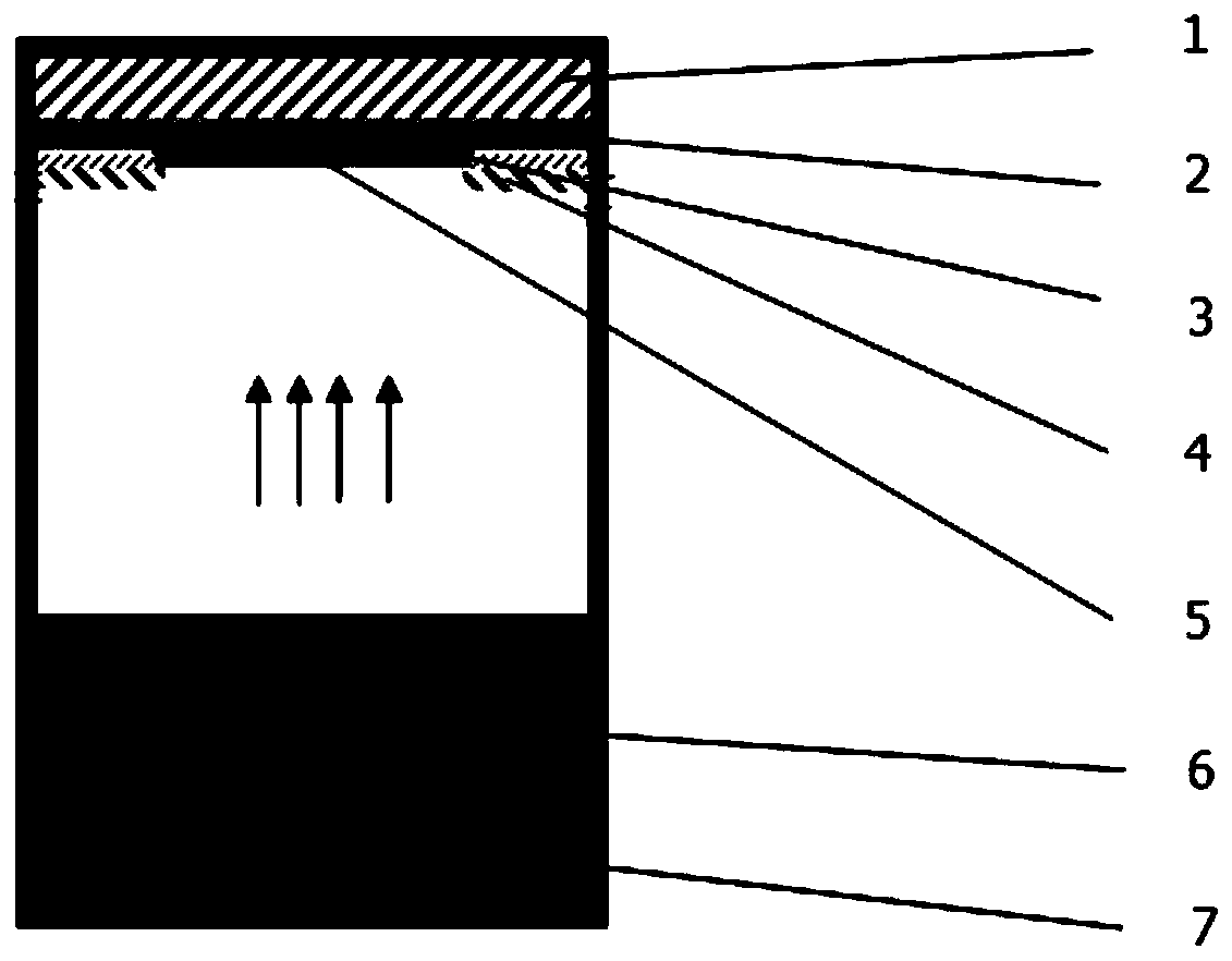
[0028] Step 1. Put the silicon carbide raw material with a purity of 99.99% into the graphite crucible, place the growth side of the seed crystal coated with carbon film on the back on the circular step of the lower layer of the graphite crucible cover, and cover it with a high-purity glass with a thickness of 10 mm. Graphite felt insulation layer, the upper layer of the graphite crucible cover and the lower layer of the graphite crucible cover are screwed tightly, and then the lower layer of the graphite crucible cover is screwed tightly with the graphite crucible cavity;

[0029] Step 2, putting the sealed graphite crucible into the crystal growth furnace, sealing the crystal growth furnace, and evacuating;

[0030] Step 3. Using the physical vapor transport method to grow silicon carbide crystals, the crystal growth temperature is 2350°C, the substrate area tempera...

Embodiment 2

[0033] A method for growing a low-stress silicon carbide single crystal, the specific preparation steps are:

[0034] Step 1. Put the silicon carbide raw material with a purity of 99.99% into the graphite crucible, place the growth side of the seed crystal coated with carbon film on the back on the circular step of the lower layer of the graphite crucible cover, and cover it with a high-purity glass with a thickness of 15 mm. Graphite felt insulation layer, the upper layer of the graphite crucible cover and the lower layer of the graphite crucible cover are screwed tightly, and then the lower layer of the graphite crucible cover is screwed tightly with the graphite crucible cavity;

[0035] Step 2, putting the sealed graphite crucible into the crystal growth furnace, sealing the crystal growth furnace, and evacuating;

[0036] Step 3. Using the physical vapor transport method to grow silicon carbide crystals, the crystal growth temperature is 2400°C, the substrate area tempera...


PUM

PropertyMeasurementUnit
depthaaaaaaaaaa
thicknessaaaaaaaaaa
warpageaaaaaaaaaa

Abstract

The invention discloses a graphite crucible device for silicon carbide crystal growth and a silicon carbide single crystal growth method thereof. The structure of the graphite crucible cover is changed, the graphite crucible cover is changed into a two-section type structure, furthermore, a seed crystal fixing mode is changed into a mechanical fixing mode from a traditional gluing mode; a carbon film is plated on the back of the seed crystal; the two-section type graphite crucible cover is screwed and fixed; a heat preservation graphite felt can be placed between the seed crystal and the upperlayer of the graphite crucible cover according to the thickness difference; high-purity silicon carbide powder is put into the graphite crucible; the sealed graphite crucible is put into a crystal growth furnace; a silicon carbide crystal is grown by adopting a physical vapor transport method; wherein the crystal growth temperature is 1950-2550 DEG C, the substrate temperature is 2200 DEG C or below, the raw material temperature is larger than 2350 DEG C, inert gas serves as carrier gas, the air pressure in the reaction chamber is 1-5 kPa, the growth time is 70 hours or longer, and the low-stress silicon carbide crystal ingot can be obtained.

Description

technical field [0001] The invention relates to a silicon carbide single crystal growth method, in particular to a graphite crucible device for silicon carbide crystal growth and a single crystal growth method thereof. Background technique [0002] Silicon carbide single crystal is a typical third-generation semiconductor material. It has the advantages of wide bandgap, strong breakdown electric field, large saturated electron drift rate, high thermal conductivity and high chemical stability. It is widely used in aerospace, communication, etc. High-power power electronic devices and optoelectronic devices in other fields can work stably for a long time in extreme environments. [0003] At present, the common method for preparing silicon carbide single crystal is physical vapor transport method, namely PVT method. The basic process is that high-purity silicon carbide powder is used as raw material and put into a high-purity graphite crucible. The silicon carbide single cryst...

Claims


Application Information

Patent Timeline
Patent Type & Authority Applications(China)
IPC IPC(8): C30B23/02C30B29/36
CPCC30B23/02C30B29/36
Inventor 李祥彪仲崇贵杨培培
Owner NANTONG UNIVERSITY
Learn More