Aluminum nitride template and preparation method thereof
An aluminum nitride and template technology, applied in semiconductor/solid-state device manufacturing, electrical components, circuits, etc., can solve problems such as wafer cracking and high defect density, and achieve the effect of reducing defect density and realizing dislocation density.
- Summary
- Abstract
- Description
- Claims
- Application Information
AI Technical Summary
Problems solved by technology
Method used
Image
Examples
preparation example Construction
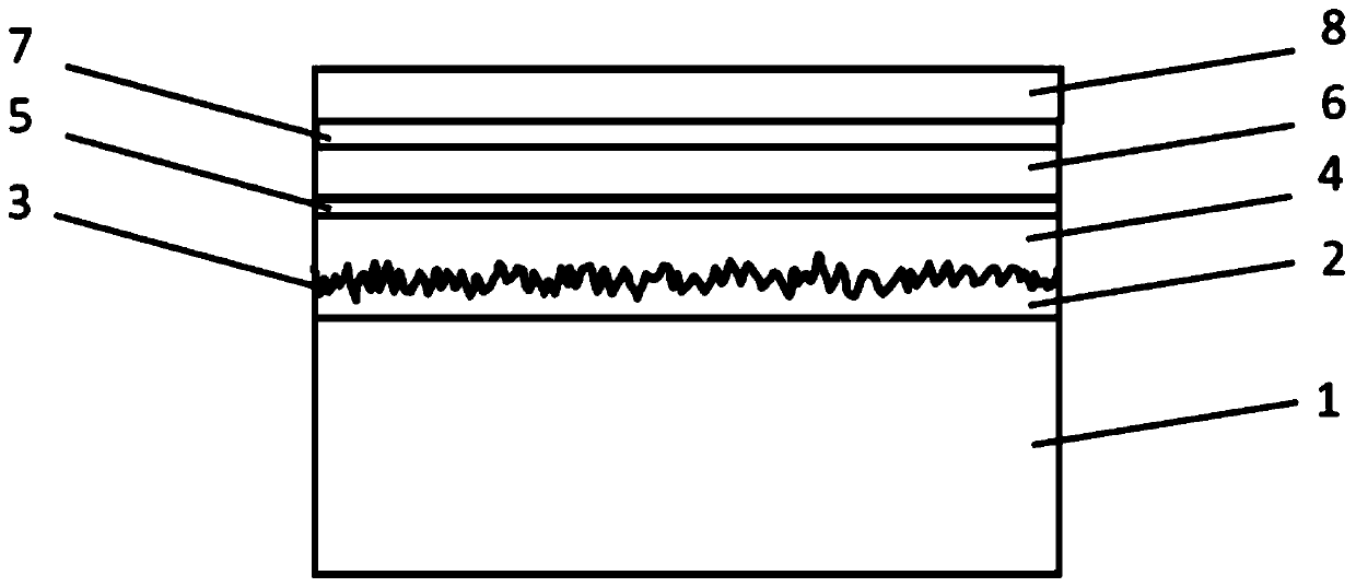
[0034] An embodiment of the present invention provides a method for preparing an aluminum nitride template, which includes:
[0035] placing the substrate in the reaction chamber, and preparing an AlN or BN buffer layer on the substrate;
[0036] An AlN epitaxial layer is prepared on the AlN or BN buffer layer, and at least a BAlN insertion layer is prepared and formed in the AlN epitaxial layer, thereby forming the aluminum nitride template.
[0037] In some more specific embodiments, the preparation method includes: introducing a nitrogen source and an aluminum source into the reaction chamber, and growing an AlN buffer layer on the substrate at 1400-1500°C; or, injecting the A nitrogen source and a boron source are fed into the reaction chamber, and a BN buffer layer is grown on the substrate under the condition of 1400-1500°C.
[0038] In some more specific embodiments, the preparation method includes: introducing a nitrogen source and an aluminum source into the reaction...
Embodiment 1
[0058] A method for preparing an aluminum nitride template may comprise the steps of:
[0059] 1) Place the sapphire or SiC substrate in a CVD (Chemical Vapor Deposition) or HVPE (Hydride Vapor Phase Epitaxy) reaction chamber, and raise the temperature in the reaction chamber to 1400-1600°C, and then inject hydrogen into the reaction chamber Cleaning sapphire or SiC substrates;
[0060] 2) Feed a nitrogen source and an aluminum source into the reaction chamber, and grow an AlN buffer layer with a thickness of 500-2000nm at a temperature of 1400-1500°C;
[0061] 3) After the growth of the AlN buffer layer is completed, stop feeding the aluminum source, and adjust the temperature in the reaction chamber to 1400-1550°C;
[0062] 4) Feed an aluminum source into the reaction chamber at 1400-1550° C. to grow an AlN epitaxial layer in situ on the AlN buffer layer;
[0063] 5) Maintain the growth conditions of the AlN epitaxial layer (1400-1550 ° C), feed the boron source into the r...
Embodiment 2
[0067] A method for preparing an aluminum nitride template may also include the following steps:
[0068] 1) Place the sapphire or SiC substrate in a CVD (Chemical Vapor Deposition) or HVPE (Hydride Vapor Phase Epitaxy) reaction chamber, and raise the temperature in the reaction chamber to 1400-1600°C, and then inject hydrogen into the reaction chamber Cleaning sapphire or SiC substrates;
[0069] 2) Feed a nitrogen source and a boron source into the reaction chamber, and grow a BN buffer layer with a thickness of 500-2000nm at a temperature of 1400-1500°C;
[0070] 3) After the growth of the BN buffer layer is completed, the boron source is stopped, and the temperature in the reaction chamber is adjusted to 1400-1550° C.;
[0071] 4) Feed an aluminum source into the reaction chamber at 1400-1550° C. to grow an AlN epitaxial layer in situ on the BN buffer layer;
[0072] 5) Maintain the growth conditions of the AlN epitaxial layer (1400-1550 ° C), feed the boron source into ...
PUM
| Property | Measurement | Unit |
|---|---|---|
| Thickness | aaaaa | aaaaa |
| Thickness | aaaaa | aaaaa |
| Thickness | aaaaa | aaaaa |
Abstract
Description
Claims
Application Information


