Monocrystalline silicon wafer, monocrystalline silicon rod, preparation method of monocrystalline silicon rod, solar cell and assembly

A technology for solar cells and monocrystalline silicon wafers, applied in electrical components, circuits, photovoltaic power generation, etc., can solve problems such as inconsistent angles, asymmetric arc angles, and easy misalignment, and achieve consistent and controllable grinding arcs. The effect of good consistency and avoiding misalignment

Pending Publication Date: 2020-07-31
天津市环智新能源技术有限公司
View PDF0 Cites 0 Cited by
  • Summary
  • Abstract
  • Description
  • Claims
  • Application Information

AI Technical Summary

Problems solved by technology

[0002] At present, the shape of the four corners of silicon wafers for solar energy is generally arc corners, such as figure 1 As shown, the corners of this shape can effectively reduce stress concentration and reduce the fragmentation of silicon wafers during transportation and processing. The accuracy and positioning requirements are getting higher and higher. This kind of arc-shaped structure is difficult to meet the positioning requirements of downstream battery electrode printing and battery assembly assembly, that is, the positioning effect of this kind of arc-shaped structure is poor when positioning through arc angles, for example , when splicing two arc-shaped single crystal silicon wafers on the same plane, it is easy to dislocate
[0003] In addition, there are following defects in the process from single crystal silicon rods to single crystal silicon wafers with arc-shaped structure: the grinding process in the prior art is as follows figure 2 As shown, among them, v1 is the feeding direction of the silicon rod, v2 is the rotation direction of the single crystal silicon rod, and v3 is the rotation direction of the grinding wheel. When grinding, the single crystal silicon rod and the grinding wheel rotate simultaneously, so that the four single crystal silicon rods The consistency of the edge grinding arc is difficult to control. When the arc angle gradually decreases, due to the problem of tool accuracy in the processing process, there will be inconsistencies in the angles of the entry and exit of the knife, resulting in the asymmetry of the arc angle.
Generally, there is more wear at the entry point, and less wear at the exit point, that is, some edges and corners are over-polished, and some corners are not polished, which affects the yield of monocrystalline silicon wafers.

Method used


Image

  • Monocrystalline silicon wafer, monocrystalline silicon rod, preparation method of monocrystalline silicon rod, solar cell and assembly
  • Monocrystalline silicon wafer, monocrystalline silicon rod, preparation method of monocrystalline silicon rod, solar cell and assembly
  • Monocrystalline silicon wafer, monocrystalline silicon rod, preparation method of monocrystalline silicon rod, solar cell and assembly

Examples


preparation example Construction

[0055] A method for preparing a single crystal silicon rod, for preparing the above-mentioned single crystal silicon rod, such as Figure 4 shown, including the following steps,

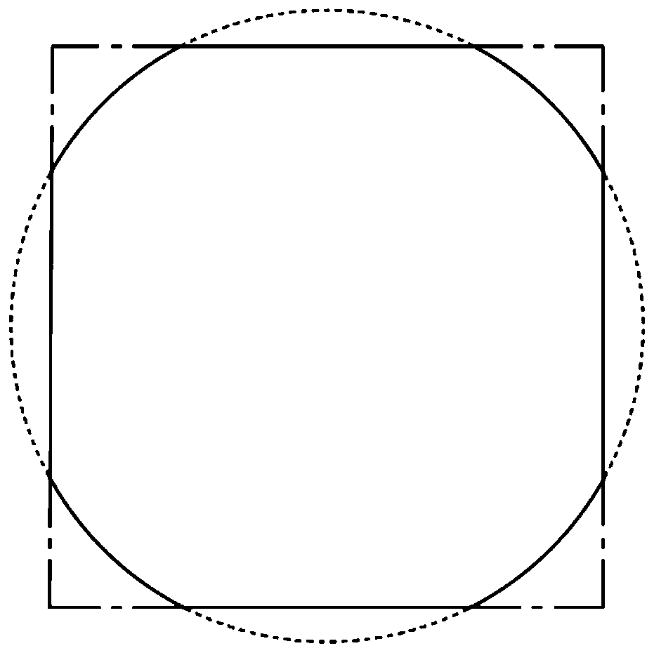
[0056] Square the single wafer rod to form a plurality of first straight wall parts and multiple edge parts: use a diamond wire to cut the single wafer rod formed by Czochralski single crystal, remove the edge skin of the single wafer rod, and form The polygonal cylinder has a plurality of first straight wall parts and edge parts, and the number of the first straight wall parts is selected according to actual needs, and no specific requirements are set here. When the number of the first straight wall parts is four, the single wafer bar is cut to form a square bar with a cuboid structure.

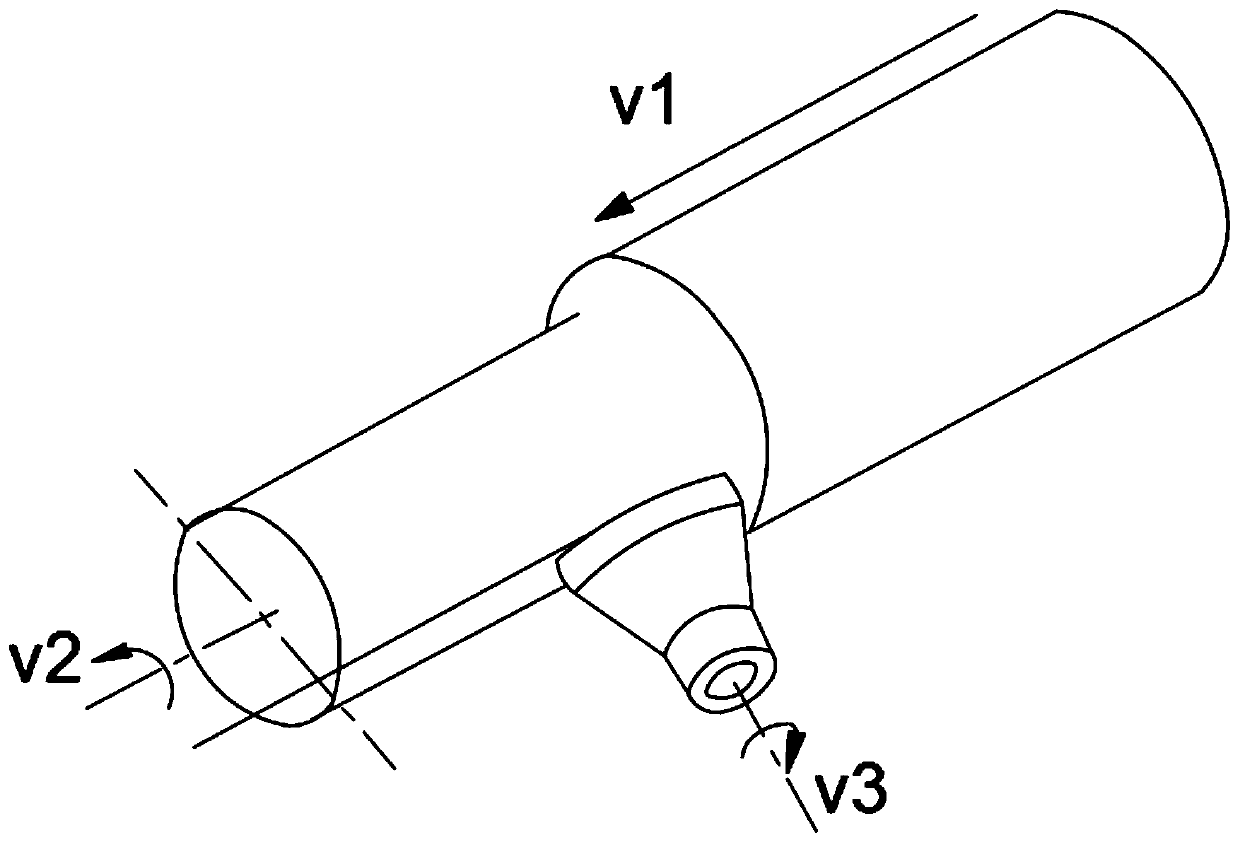
[0057] Chamfer the edges of the squared single-wafer rod. When chamfering the edges, use a grinding wheel to grind the edges, such as Figure 4 As shown in the figure, v1 is the feeding direction of the silicon r...

Embodiment 1

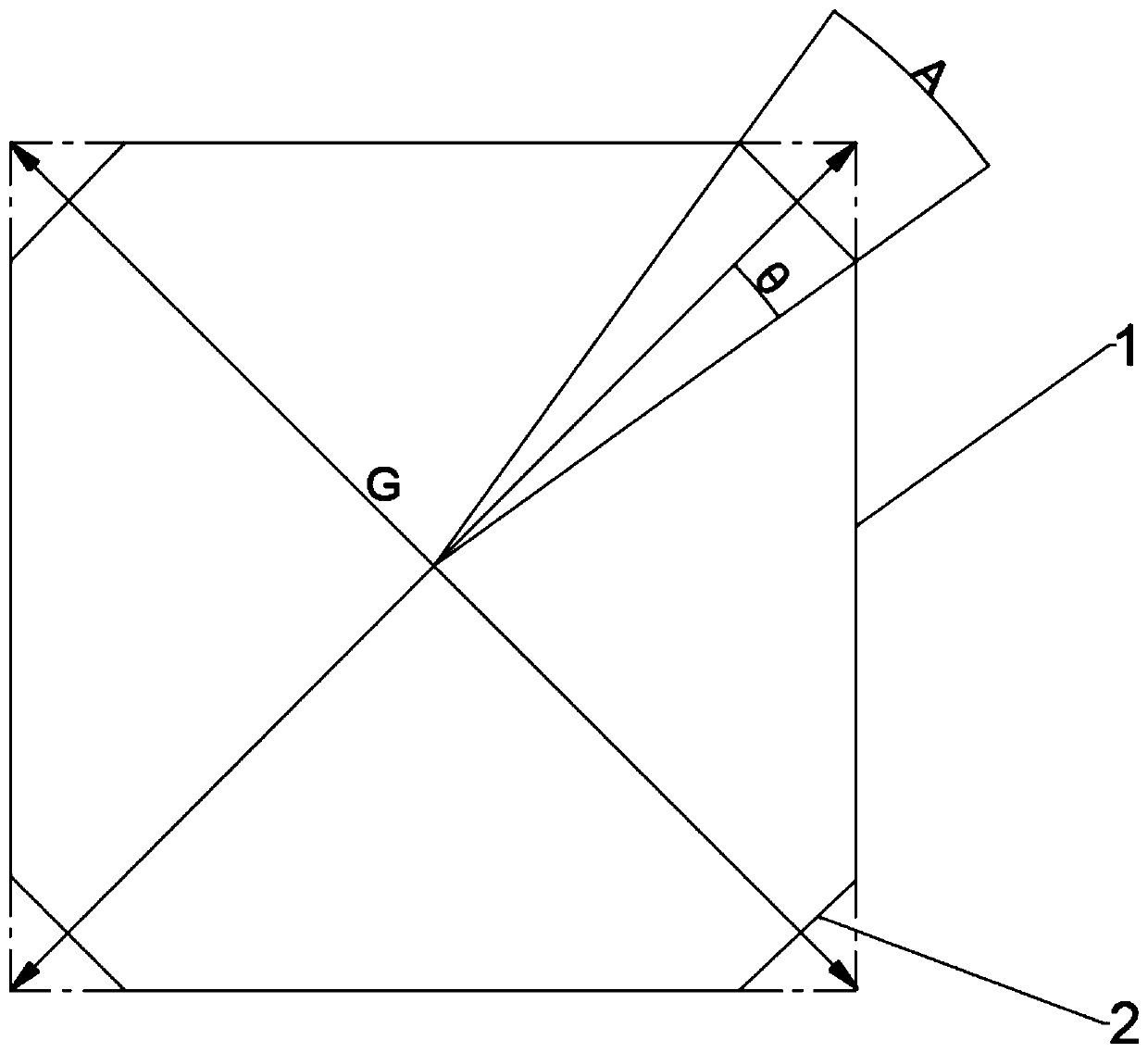
[0064] A single crystal silicon wafer, comprising a silicon wafer body, the silicon wafer body includes a plurality of straight wall parts 1 and a plurality of chamfered parts 2, the straight wall parts 1 and the chamfered parts 2 are connected end to end alternately in sequence, and the chamfered parts 2 are straight lines type, the length of the chamfered part 2 is 1.53mm, the end point of either end of the chamfered part 2 of the silicon wafer body and the center point of the silicon wafer body are connected to the line formed by the crystal direction of the silicon wafer body The angle of the included angle is 0.33 °, the angle of the central angle A corresponding to the center of the chamfering portion 2 and the silicon wafer body is 0.65 °, and the center line of the central angle A coincides with the diagonal line G of the silicon wafer body, then it is assumed that the Half of the central angle A is θ, and the crystal orientation in the thickness direction of the silic...

Embodiment 2

[0071] A single crystal silicon wafer, comprising a silicon wafer body, the silicon wafer body includes a plurality of straight wall parts 1 and a plurality of chamfered parts 2, the straight wall parts 1 and the chamfered parts 2 are connected end to end alternately in sequence, and the chamfered parts 2 are straight lines type, the length of the chamfered part 2 is 10mm, the end point of either end of the chamfered part 2 of the silicon wafer body is connected with the center point of the silicon wafer body, and the line formed by the connection between the crystal direction of the silicon wafer body The angle of the corner is 3.2 °, the angle of the central angle A corresponding to the center of the chamfering part 2 and the center of the silicon wafer body is 6.4 °, and the center line of the central angle A coincides with the diagonal line G of the silicon wafer body, then the center Half of the angle A is θ, and the crystal orientation in the thickness direction of the sil...


PUM

PropertyMeasurementUnit
Lengthaaaaaaaaaa
Lengthaaaaaaaaaa
Lengthaaaaaaaaaa

Abstract

The invention provides a monocrystalline silicon wafer. The monocrystalline silicon wafer comprises a silicon wafer body, the silicon wafer body comprises a plurality of straight wall parts and a plurality of chamfer parts, the straight wall parts and the chamfering parts are sequentially and alternately connected end to end, the chamfering parts are linear, and the included angle between a straight line formed by connecting the end point of any end of each chamfering part and the center point of the silicon wafer body and the crystal direction of the silicon wafer body (110) is not smaller than 0.35 degree and not larger than 3.2 degrees. The monocrystalline silicon wafer has the beneficial effects that the monocrystalline silicon wafers are provided with the chamfering parts, and the chamfering parts are linear, so that the poor positioning effect of the monocrystalline silicon wafers during downstream battery electrode printing and battery assembly assembling is avoided, and the dislocation phenomenon occurring during monocrystalline silicon wafer splicing is avoided; and meanwhile, in the preparation process of the monocrystalline silicon rod, the polishing mode that the monocrystalline silicon rod does not rotate and the polishing grinding wheel rotates is adopted, so that the consistency of the corner angle polishing radian of the monocrystalline silicon rod is good.

Description

technical field [0001] The invention belongs to the technical field of silicon chip production, and in particular relates to a single crystal silicon chip, a single crystal silicon rod and a preparation method thereof, a solar battery and components. Background technique [0002] At present, the shape of the four corners of silicon wafers for solar energy is generally arc corners, such as figure 1 As shown, the corners of this shape can effectively reduce stress concentration and reduce the fragmentation of silicon wafers during transportation and processing. The accuracy and positioning requirements are getting higher and higher. This kind of arc-shaped structure is difficult to meet the positioning requirements of downstream battery electrode printing and battery assembly assembly, that is, the positioning effect of this kind of arc-shaped structure is poor when positioning through arc angles, for example , When splicing two arc-shaped single crystal silicon wafers on the...

Claims


Application Information

Patent Timeline
IPC IPC(8): H01L21/02H01L31/18B24B9/06B24B47/12B24B47/20B28D5/04
CPCB24B9/065B24B47/12B24B47/20B28D5/045H01L21/02013H01L21/02021H01L31/1804Y02E10/547Y02P70/50
Inventor 沈浩平李建弘危晨刘涛赵越
Owner 天津市环智新能源技术有限公司
Why Eureka
Try Eureka