Novel three-dimensional silicon structure supercapacitor electrode material and preparation method thereof

A technology for supercapacitors and electrode materials, which is applied in the manufacture of hybrid capacitor electrodes and hybrid/electric double-layer capacitors, etc., can solve the problems of high manufacturing cost, complex preparation steps, and complicated processes, and achieve process compatibility, cost reduction, low cost, etc. The effect of internal resistance

Active Publication Date: 2020-08-07
JIANGSU UNIV
View PDF5 Cites 0 Cited by
  • Summary
  • Abstract
  • Description
  • Claims
  • Application Information

AI Technical Summary

Problems solved by technology

At present, based on this structure, researchers at home and abroad have prepared a series of silicon-based supercapacitors, but the preparation steps are relatively complicated. During the preparation process, CVD, ALD, or high-temperature calcination may be used to passivate the silicon. The surface, the process is more complicated, and the production cost is relatively high

Method used


Image

  • Novel three-dimensional silicon structure supercapacitor electrode material and preparation method thereof
  • Novel three-dimensional silicon structure supercapacitor electrode material and preparation method thereof
  • Novel three-dimensional silicon structure supercapacitor electrode material and preparation method thereof

Examples


Embodiment 1

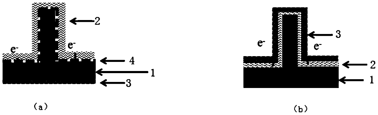
[0029] (1) Silicon nanowires (SiNWs) were prepared by solution etching, and treated twice to prepare a silicon substrate with a three-dimensional surface structure.

[0030] (a) Select N-type (100 crystal orientation), single-sided polished silicon wafer with a resistivity of 5-7Ω cm, cut into 1cm*2cm samples, wash with ethanol and deionized water for many times; Put it into the etching solution containing 5mol / L and 0.02mol / L silver nitrate and etch for 60min.

[0031] (b) Soak the silicon wafer in a concentrated nitric acid solution for more than 1 hour to remove the residual silver particles on the surface of the silicon nanowires, then fully wash it with deionized water, and dry it at a high speed with a homogenizer.

[0032] (c) The silicon wafer is immersed in a chlorobenzene saturated solution of phosphorus pentachloride for secondary treatment. The treatment time is 3 hours, and the treatment temperature is 120° C.

[0033] (2) Spin-coat 3 layers of PEDOT:PSS solution...

Embodiment 2

[0037] (1) Silicon nanowires (SiNWs) were prepared by solution etching, and treated twice to prepare a silicon substrate with a three-dimensional surface structure.

[0038] (a) Select N-type (100 crystal orientation), single-sided polished silicon wafer with a resistivity of 5-7Ω cm, cut into 1cm*2cm samples, wash with ethanol and deionized water for many times; Put it into the etching solution containing 5mol / L and 0.02mol / L silver nitrate and etch for 60min.

[0039] (b) Soak the silicon wafer in a concentrated nitric acid solution for more than 1 hour to remove the residual silver particles on the surface of the silicon nanowires, then fully wash it with deionized water, and dry it at a high speed with a homogenizer.

[0040] (c) The silicon wafer is immersed in a chlorobenzene saturated solution of phosphorus pentachloride for secondary treatment. The treatment time is 3 hours, and the treatment temperature is 120° C.

[0041] (2) Spin-coat 3 layers of PEDOT:PSS solution...

Embodiment 3

[0047] (1) Silicon nanowires (SiNWs) were prepared by solution etching, and treated twice to prepare a silicon substrate with a three-dimensional surface structure.

[0048] (a) N-type (100 crystal orientation), single-sided polished silicon wafer with a resistivity of 5-7Ω·cm, cut into 1cm*2cm samples, washed with ethanol and deionized water for many times; at room temperature and pressure Put it into the etching solution containing 5mol / L and 0.02mol / L silver nitrate and etch for 60min.

[0049] (b) Soak the silicon wafer in a concentrated nitric acid solution for more than 1 hour to remove the residual silver particles on the surface of the silicon nanowires, then fully wash it with deionized water, and dry it at a high speed with a homogenizer.

[0050] (c) The silicon wafer is immersed in a chlorobenzene saturated solution of phosphorus pentachloride for secondary treatment. The treatment time is 3 hours, and the treatment temperature is 120° C.

[0051] (2) Spin-coat 3 ...


PUM

PropertyMeasurementUnit
electrical resistivityaaaaaaaaaa
thicknessaaaaaaaaaa
concentrationaaaaaaaaaa

Abstract

The invention provides a novel three-dimensional silicon structure supercapacitor electrode material and a preparation method thereof. The method comprises the steps: taking a three-dimensional silicon structure as a substrate, preparing an active layer on the surface of the substrate, and enabling a charge collection layer to cover the surface of the active layer, wherein the porous network-shaped charge collection layer with relatively high conductivity is prepared on the surface of the active layer by taking a two-dimensional conductive material of a charge collection layer as a main body and a conductive polymer as a binder. According to the invention, when a large-area electrode material is prepared, a metal gate electrode material is evaporated on the surface of a high-conductivity layer in order to improve the charge collection efficiency; and the three-dimensional silicon structure electrode material prepared by the method does not need to consider the conductivity, the purityand the crystal form of the silicon substrate, and does not need to passivate the silicon surface, so that the raw material cost of the silicon electrode material is reduced, and the preparation method of the silicon electrode is simplified.

Description

technical field [0001] The invention belongs to the field of electrode materials, and relates to a novel three-dimensional silicon structure supercapacitor electrode material and a preparation method thereof. Background technique [0002] From aeronautics to biomedicine, the emergence of innovative miniature portable devices, such as wireless microsensors or biomedical implantable microdevices, has aroused great interest in the field of energy storage devices. The technical specifications of such micro-devices require high-performance small-sized power supplies, including high power density and energy density, as well as long life and good compatibility with the microelectronics industry. As the second most abundant element on earth, silicon is the most thoroughly studied element among all chemical elements. At the same time, most semiconductor components are prepared from silicon. Silicon materials are used in optoelectronics, microelectronics and other industries occupy a...

Claims


Application Information

Patent Timeline
Patent Type & Authority Applications(China)
IPC IPC(8): H01G11/24H01G11/26H01G11/46H01G11/48H01G11/86
CPCH01G11/24H01G11/26H01G11/46H01G11/86H01G11/48Y02E60/13
Inventor 申小娟张旋朱脉勇李松军
Owner JIANGSU UNIV
Why Eureka
Try Eureka