Preparation method of stable silicon-coated pure-phase CsPb2Br5 inorganic nanocrystal

An inorganic nano- and silicon-coated technology, which is applied in the field of preparation of pure-phase CsPb2Br5 inorganic nanocrystals, can solve the problems of loss of stability, surface detachment of surface ligand oleylamine, etc. Effect

Active Publication Date: 2020-08-11
UNIV OF ELECTRONIC SCI & TECH OF CHINA
View PDF6 Cites 3 Cited by
  • Summary
  • Abstract
  • Description
  • Claims
  • Application Information

AI Technical Summary

Problems solved by technology

Miscellaneous CsPbBr can be effectively removed by the purification process 3 nanocrystals, but multiple purification processes l

Method used


Image

  • Preparation method of stable silicon-coated pure-phase CsPb2Br5 inorganic nanocrystal
  • Preparation method of stable silicon-coated pure-phase CsPb2Br5 inorganic nanocrystal
  • Preparation method of stable silicon-coated pure-phase CsPb2Br5 inorganic nanocrystal

Examples


Embodiment 1

[0020] This example provides a stable silicon-coated pure-phase CsPb 2 Br 5 The preparation method of inorganic nanocrystal specifically comprises the following steps:

[0021] Step 1, in the round bottom flask of 50mL, add 0.1mmol cesium carbonate (Cs 2 CO 3 ) with 0.3mmol anhydrous lead acetate (Pb(Ac) 2 ), then add 5mL octadecene (ODE), 2.8mmol oleic acid (OA) and 2.9mmol 3-aminopropyltriethoxysilane (APTES) to prepare a reaction precursor solution;

[0022] Step 2. Place the flask containing the reaction precursor solution in a magnetic heating stirrer with a rotation speed of 1000rpm, and connect the double-row tubes that can switch nitrogen and vacuum environments. First, the reaction precursor solution is raised to 60°C, switch nitrogen three times; then switch back to vacuum conditions, raise the temperature to 90°C, switch nitrogen three times again; then continue to heat up to 120°C under vacuum conditions and keep it warm for 20 minutes. 2 CO 3 and Pb(Ac) 2 A...

Embodiment 2

[0026] Prepare stable silicon-coated pure-phase CsPb according to the steps of Example 1 of the present invention 2 Br 5 Inorganic nanocrystals, the difference is that only the amount of anhydrous lead acetate in step 1 is adjusted to 0.4 mmol, and the other steps remain unchanged.

Embodiment 3

[0028]Prepare stable silicon-coated pure-phase CsPb according to the steps of Example 2 of the present invention 2 Br 5 For inorganic nanocrystals, the difference is that only the last heating temperature in step 2 is adjusted to 150° C., and other steps remain unchanged.

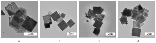
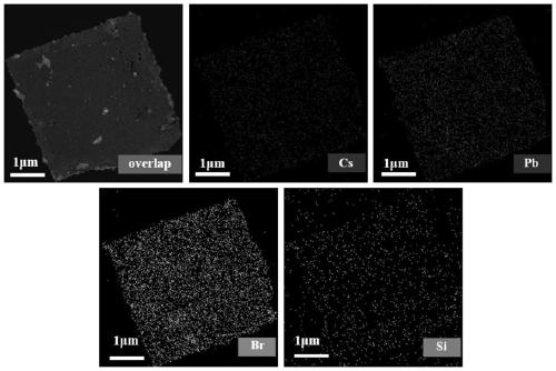
[0029] To illustrate the effect of different purification times on silicon-coated CsPb 2 Br 5 Influence of the purity of nanocrystals, Example 1 of the present invention prepared silicon-coated CsPb purified 1, 3, 5 and 7 times respectively 2 Br 5 nanocrystals, made of figure 1 The TEM image shown shows that after purification once, CsPb 2 Br 5 There are still a lot of CsPbBr mixed in the nanocrystals (square nanosheets) 3 Nanocrystalline (small particles at the edge), with the increase of purification times, CsPbBr 3 The nanocrystals gradually decreased, and after 7 times of purification, the CsPbBr 3 disappear, resulting in pure phase CsPb coated with Si 2 Br 5 Nanocrystalline.
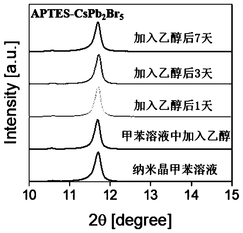
[0030] Depend...


PUM


Abstract

The invention provides a preparation method of a stable silicon coated pure-phase CsPb2Br5 inorganic nanocrystal. The preparation method comprises the following steps: adding octadecene, oleic acid and APTES into cesium carbonate and anhydrous lead acetate to prepare a reaction precursor solution, performing heating and stirring, performing heating to 60 DEG C under vacuum, and introducing nitrogen to remove reaction gas generated in the heating process; cutting back to vacuum, heating to 90 DEG C, and introducing nitrogen; heating to 120 DEG C in vacuum, keeping the temperature until cesium carbonate and anhydrous lead acetate are completely dissolved, introducing nitrogen, heating to 140-150 DEG C, injecting trimethylbromosilane, reacting for 1 hour, and cooling to room temperature; andperforming mixing with methyl acetate, and purifying the mixture for seven times to obtain the stable silicon-coated pure-phase CsPb2Br5 nanocrystal. According to the method, a silicon shell layer isprepared by adopting APTES, the stability of the nanocrystal is improved, the structure of the silicon shell layer is not damaged after multiple times of purification, and the high stability is achieved while it is guaranteed that the pure-phase CsPb2Br5 nanocrystal is synthesized.

Description

technical field [0001] The invention belongs to the technical field of semiconductor nanomaterial preparation, in particular to pure phase CsPb coated with stable silicon 2 Br 5 Preparation methods of inorganic nanocrystals. Background technique [0002] Perovskite nanocrystals (PNCs) are particles with a size close to the exciton Bohr radius, which have the advantages of high absorption coefficient, high carrier mobility, and shallow defect energy levels of perovskite materials. It also has unique advantages such as diverse morphology, quantum size effect, high photoluminescence quantum yield, and narrow emission linewidth of nanomaterials. Its photoelectric properties are closely related to synthesis temperature, surface ligand density, and precursor concentration. The emission wavelengths covering the entire visible light range can be obtained by sub-tuning. In recent years, PNCs have been widely used in the field of optoelectronics due to their excellent optical prope...

Claims


Application Information

Patent Timeline
IPC IPC(8): C01G21/00B82Y40/00B82Y30/00
CPCB82Y30/00B82Y40/00C01G21/006C01P2002/72C01P2004/04C01P2004/80
Inventor 刘明侦卫林峰曾鹏赵海峰
Owner UNIV OF ELECTRONIC SCI & TECH OF CHINA
Why Eureka
Try Eureka