Three-terminal type thin film transistor, preparation method thereof and photosensitive nerve synapse device

A thin-film transistor and oxide thin-film technology, which is applied in the field of optoelectronic devices, can solve the problems that photosensitive synapses do not have obvious advantages and the oxide band gap is large, and achieve the effects of low power consumption and simple preparation methods

Inactive Publication Date: 2020-08-18
NINGBO INST OF MATERIALS TECH & ENG CHINESE ACADEMY OF SCI
View PDF4 Cites 5 Cited by
  • Summary
  • Abstract
  • Description
  • Claims
  • Application Information

AI Technical Summary

Problems solved by technology

[0005] However, due to the large band gap of oxides, the corresponding light absorption wavelengths are generally concentrated in the ultraviolet band, and as the wavelengt...

Method used


Image

  • Three-terminal type thin film transistor, preparation method thereof and photosensitive nerve synapse device
  • Three-terminal type thin film transistor, preparation method thereof and photosensitive nerve synapse device
  • Three-terminal type thin film transistor, preparation method thereof and photosensitive nerve synapse device

Examples


Embodiment 1

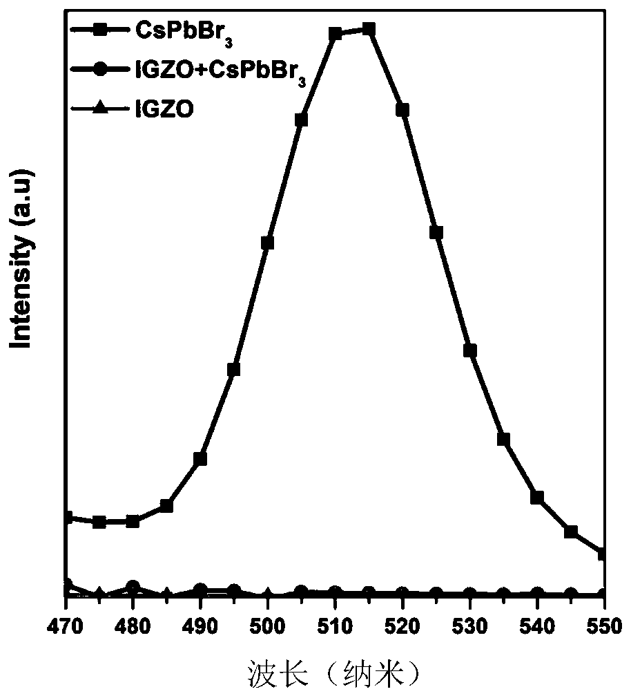
[0040] Spin-coat CsPbBr with toluene as solvent on quartz glass plate A 3 -QDs solution, then heated to volatilize toluene to obtain CsPbBr with a thickness of 20nm 3 -QDs quantum dot layer;

[0041] Using radio frequency magnetron sputtering technology, grow an indium gallium zinc oxide film (IGZO film) with a thickness of 50 nm on the quartz glass sheet B;

[0042] First, an IGZO film with a thickness of 20 nm was grown on a quartz glass sheet C by radio frequency magnetron sputtering technology, and then CsPbBr with toluene as a solvent was spin-coated on the IGZO film. 3 -QDs solution, heated to volatilize toluene to obtain CsPbBr with a thickness of 20nm 3 -QDs layer, finally in CsPbBr by RF magnetron sputtering 3 - growing an IGZO thin film with a thickness of 30 nm on the QDs layer to obtain a composite thin film layer of IGZO thin film / quantum dots.

[0043] The three types of samples on the quartz glass sheets A, B, and C were analyzed and characterized by a fluores...

Embodiment 2

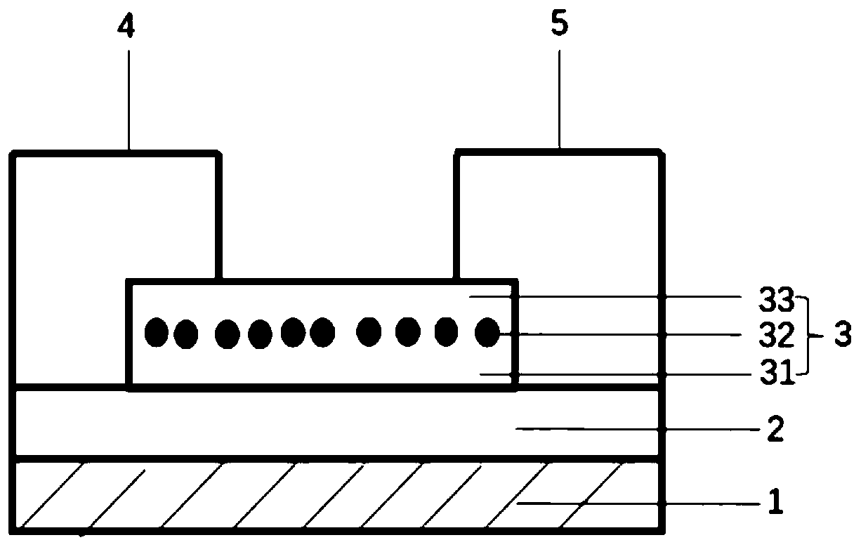
[0045] Thin film transistor structures such as figure 1 As shown, it includes a substrate, a channel layer 3 , a gate electrode, a source electrode 4 and a drain electrode 5 . Wherein, the gate electrode is located in one layer of the channel layer, and the source electrode 4 and the drain electrode 5 are located in the other layer of the channel layer 3, forming a dislocation structure.

[0046] In this embodiment, a p-type doped Si material 1 (p+Si for short) is selected as the substrate and the gate electrode, and SiO grown by thermal oxidation is arranged between the channel layer 3 and the gate electrode. 2 as the gate insulating layer 2.

[0047] In this embodiment, the material of the source electrode 4 is an alloy of Ti and Au, and the material of the drain electrode 5 is an alloy of Ti and Au.

[0048] In this embodiment, the channel layer 3 is made of the first indium gallium zinc oxide thin film layer 31 (first IGZO thin film layer 31), CsPbBr 3 Quantum dot layer...
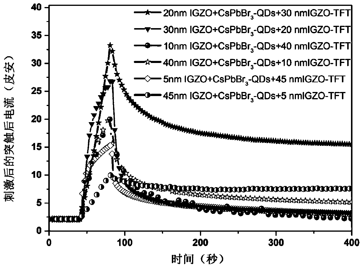
Embodiment 3-9

[0060] In Examples 3-9, the structure of the thin film transistor is basically the same as that in Example 2, and the different thicknesses of the first IGZO thin film layer and the second IGZO thin film layer are shown in the table below.

[0061] In the embodiment 3-9, the preparation method of the thin film transistor is basically the same as the preparation method of the thin film transistor in the embodiment 2, and the different sputtering time when preparing the first IGZO thin film layer and the second IGZO thin film layer is shown in the following table .

[0062] Table 1

[0063]

[0064]


PUM

PropertyMeasurementUnit
Thicknessaaaaaaaaaa
Thicknessaaaaaaaaaa
Thicknessaaaaaaaaaa

Abstract

The invention discloses a three-terminal type thin film transistor, a preparation method thereof and a photosensitive nerve synapse device. The three-terminal type thin film transistor comprises a substrate, a channel, a gate electrode, a source electrode and a drain electrode, wherein the channel is formed by compounding a metal oxide and a quantum dot material, and the quantum dot material is mixed in the metal oxide. The thin film transistor has the characteristics of high visible light response intensity and strong continuous photoconductive effect, so that the response spectrum of the photosensitive nerve synapse is broadened, the use requirements of the photosensitive nerve synapse in the visible light band can be met, and the thin film transistor is more suitable for being used as aphotosensitive nerve synapse device compared with the traditional oxide thin film transistor.

Description

technical field [0001] The invention relates to the technical field of optoelectronic devices, in particular to a three-terminal thin film transistor, a preparation method thereof and a photosensitive neural synapse device. Background technique [0002] With the rapid development of science and technology, the computing system based on the traditional von Neumann configuration cannot effectively solve high-complexity problems. On the contrary, the human brain not only has the advantages of low energy consumption and self-learning, but also has the characteristics of highly parallel information storage and processing. Neuron is the basic unit of brain cognition and information processing. Synapse, as the basic structure connecting two neurons, is the key to learning and performing memory functions. Based on this, it is important to design synaptic electronic devices to simulate brain-like computing. very necessary. [0003] Most of the current synaptic devices are based on ...

Claims


Application Information

Patent Timeline
IPC IPC(8): H01L31/113H01L31/0328H01L31/18G06N3/063
CPCH01L31/1136H01L31/0328H01L31/18G06N3/063Y02P70/50
Inventor 曹鸿涛段宏筱梁凌燕
Owner NINGBO INST OF MATERIALS TECH & ENG CHINESE ACADEMY OF SCI
Why Eureka
Try Eureka