Low-voltage multifunctional charge trapping synaptic transistor and preparation method thereof

A charge trapping and transistor technology, applied in the field of charge trapping synaptic transistors, can solve the problems of high operating voltage, single function, lack of simulation of short-term plasticity, etc., and achieve the effect of enhancing the interface electric field and improving efficiency

Active Publication Date: 2020-08-21
PEKING UNIV
View PDF4 Cites 6 Cited by
  • Summary
  • Abstract
  • Description
  • Claims
  • Application Information

AI Technical Summary

Problems solved by technology

[0002] Neuromorphic computing is a new type of computing architecture that integrates storage and computing by simulating the computing model of a high-parallel, high-fault-tolerant, and energy-efficient biological neuromorphic system. The basis of the morphological computing system. For synaptic devices, a large number of synaptic devices have emerged, such as Resistive Random Access Memory (RRAM), Phase Change Random Access Memory (PCRAM), ion gate control Synaptic transistor (Ionic Gated Field-effect Transistor, IGFET) and charge trapping synaptic transistor (Charge Trapped Field-effect Transistor, CTFET), in which the charge trapping synaptic transistor has good CMOS process compatibility, high integration density and read Th...

Method used


Image

  • Low-voltage multifunctional charge trapping synaptic transistor and preparation method thereof
  • Low-voltage multifunctional charge trapping synaptic transistor and preparation method thereof
  • Low-voltage multifunctional charge trapping synaptic transistor and preparation method thereof

Examples


Embodiment Construction

[0042] The present invention will be described in detail below through specific examples in conjunction with the accompanying drawings.

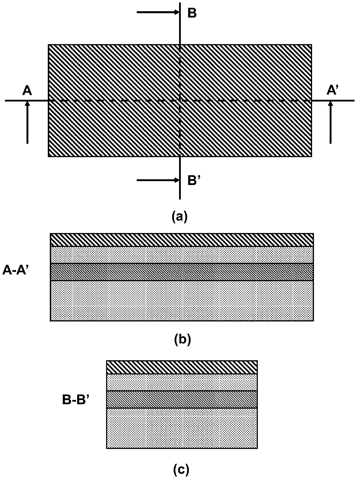
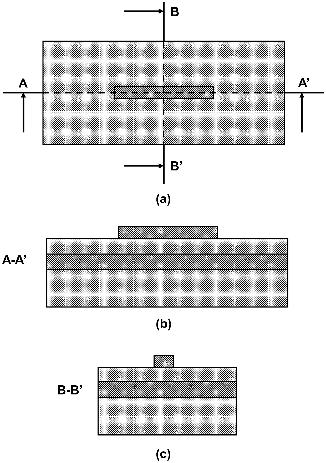
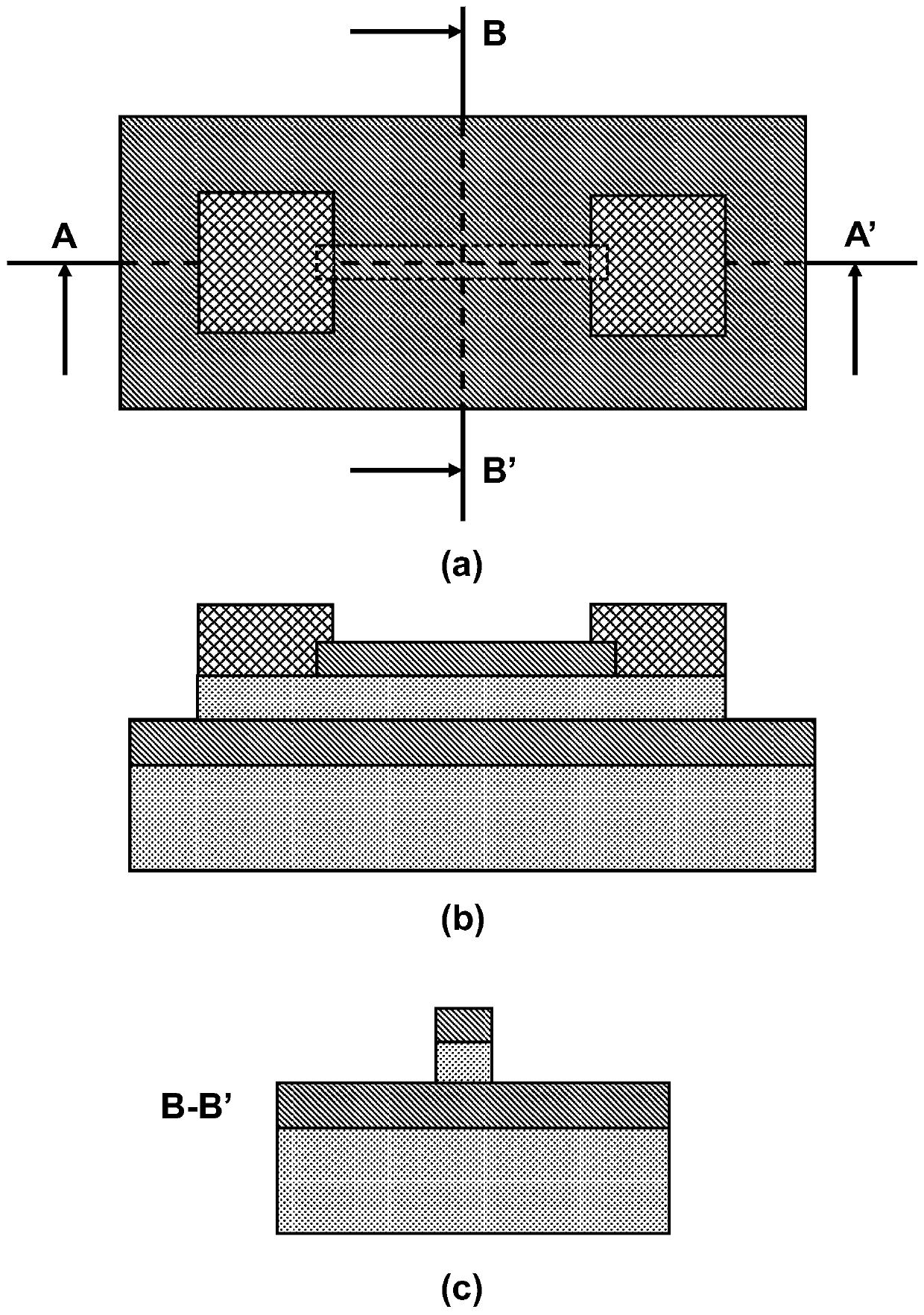
[0043] Such as Figure 1 to Figure 8 As shown, a low-voltage multifunctional charge-trapping synaptic transistor was fabricated according to the following steps:

[0044] 1) Thinning the silicon film of the SOI substrate, the specific operation method is dry oxygen oxidation or hydrogen-oxygen synthesis to oxidize the surface silicon film to form a silicon oxide film, and then rinse the surface silicon oxide film with hydrofluoric acid solution, and then spin Coated with HSQ electron beam glue, such as figure 1 shown. It is also possible to use a bulk silicon substrate, and then deposit a silicon oxide film and a polysilicon film in sequence to form an SOI substrate.

[0045] 2) Using electron beam lithography to define the nanowire mask, the width of the nanowire mask is the line width of the subsequent silicon nanowires, such as figu...


PUM

PropertyMeasurementUnit
Thicknessaaaaaaaaaa
Thicknessaaaaaaaaaa
Thicknessaaaaaaaaaa

Abstract

The invention discloses a low-voltage multifunctional charge trapping type synaptic transistor and a preparation method thereof, and belongs to the field of synaptic devices oriented to neural networkhardware application. According to the invention, a silicon nitride and hafnium oxide double-capture-layer structure is adopted to simultaneously realize short-long-time synaptic plasticity on a single device, so that the functions of the synaptic device are enriched; a three-gate nanowire structure is beneficial to enhancing an interface electric field, so that the FN tunneling width at the interface is reduced, the tunneling probability at the interface is enhanced, and the operation voltage and the device power consumption are reduced; and the device has complete CMOS material and processcompatibility, and due to the excellent device characteristics, the device has potential to be applied to a future large-scale neural network computing system.

Description

technical field [0001] The invention relates to the field of neuromorphic computing systems, provides basic synaptic device units for building neuromorphic computing systems, and particularly relates to a charge-trapping synaptic transistor with the advantages of low power consumption, high reliability and good CMOS process compatibility. Background technique [0002] Neuromorphic computing is a new type of computing architecture that integrates storage and computing by simulating the computing model of a high-parallel, high-fault-tolerant, and energy-efficient biological neuromorphic system. The basis of the morphological computing system. For synaptic devices, a large number of synaptic devices have emerged, such as Resistive Random Access Memory (RRAM), Phase Change Random Access Memory (PCRAM), ion gate control Synaptic transistor (Ionic Gated Field-effect Transistor, IGFET) and charge trapping synaptic transistor (Charge Trapped Field-effect Transistor, CTFET), in which...

Claims


Application Information

Patent Timeline
IPC IPC(8): H01L29/78H01L29/06H01L21/336H01L29/10H01L29/423
CPCH01L29/0603H01L29/1033H01L29/42356H01L29/66477H01L29/7841
Inventor 黎明李小康涂坤黄如
Owner PEKING UNIV
Why Eureka
Try Eureka