

A structure of high-voltage sic IGBT that suppresses dv/dt, di/dt noise generation
A high-voltage and noise technology, applied in the field of high-voltage power electronics, can solve the problems of increasing the thickness of the buffer layer, increasing the power loss, and limiting practical applications.
- Summary
- Abstract
- Description
- Claims
- Application Information
AI Technical Summary
Problems solved by technology
Method used
Image

Examples
Embodiment Construction
[0026] In order to make the purpose, technical solutions and advantages of the embodiments of the present invention clearer, the technical solutions in the embodiments of the present invention will be clearly and completely described below in conjunction with the drawings in the embodiments of the present invention. Obviously, the described embodiments It is a part of embodiments of the present invention, but not all embodiments. Based on the embodiments of the present invention, those of ordinary skill in the art are inspired by them, and without departing from the spirit of the invention, design structural methods and embodiments similar to the technical solution without creative design, all shall belong to this invention. The scope of patent protection.
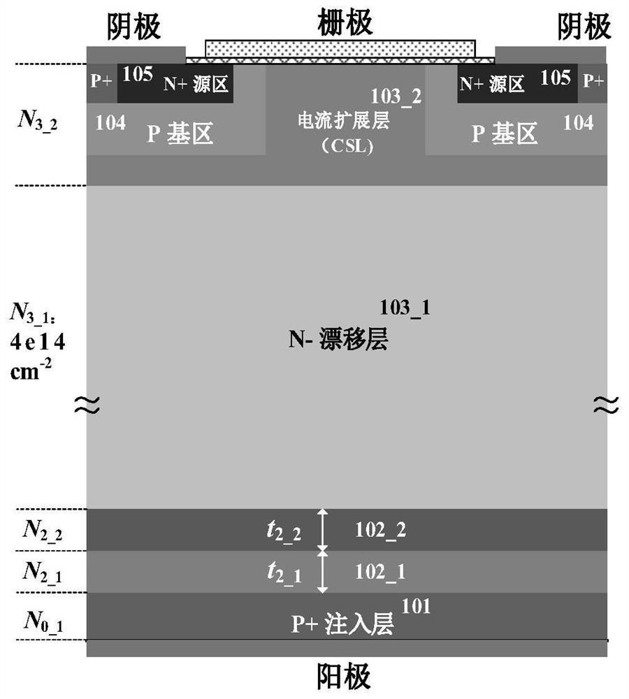
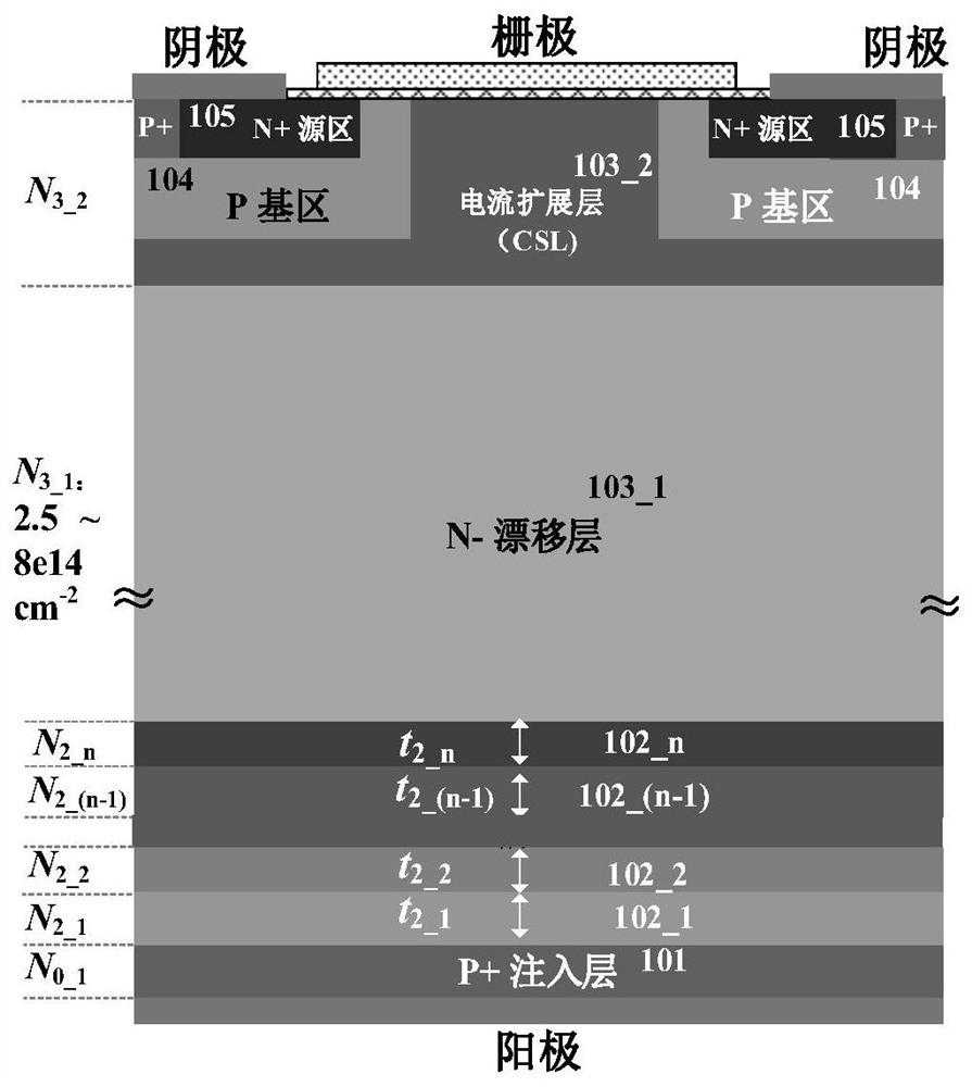
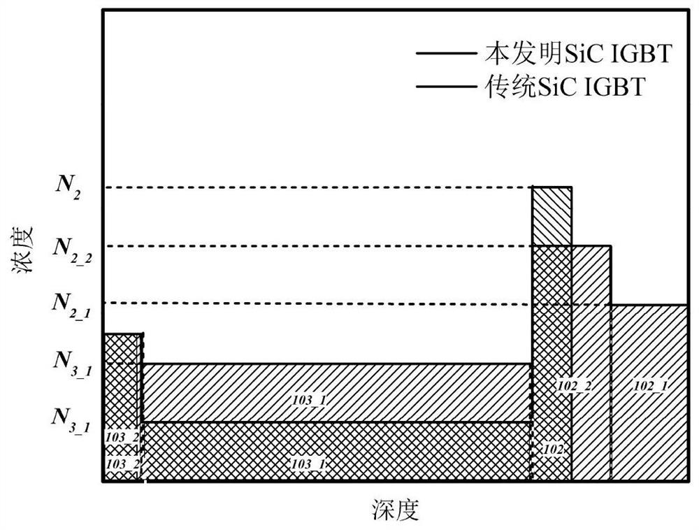
[0027] In the turn-on phase, the incomplete ionization of the P+ injection layer further reduces the current gain of the intrinsic transistor. The hole density of the channel IGBT is replenished faster, and the net charge...
PUM
 Abstract
Description
Claims
Application Information