Method for cutting metal nano structure to assemble the same into nano device and method of in-situ characterization for nano device

A technology of metal nanostructures and nanodevices, applied in the field of nanomanufacturing, can solve problems such as high equipment threshold, device pollution, and difficult control

Pending Publication Date: 2020-09-04
WUHAN UNIV
View PDF7 Cites 0 Cited by
  • Summary
  • Abstract
  • Description
  • Claims
  • Application Information

AI Technical Summary

Problems solved by technology

Although the above method can produce some nanostructures with complex configurations, it usually relies on external voltage / current or high-energy particle irradiation, which is not easy to control and easily pollutes the prepared devices.
[0004] Existing modulating the shape of metal nanostructures and preparing devices based on metal nanostructures have problems such as high equipment threshold, difficult process control, and easy pollution.

Method used


Image

  • Method for cutting metal nano structure to assemble the same into nano device and method of in-situ characterization for nano device
  • Method for cutting metal nano structure to assemble the same into nano device and method of in-situ characterization for nano device
  • Method for cutting metal nano structure to assemble the same into nano device and method of in-situ characterization for nano device

Examples


Embodiment 1

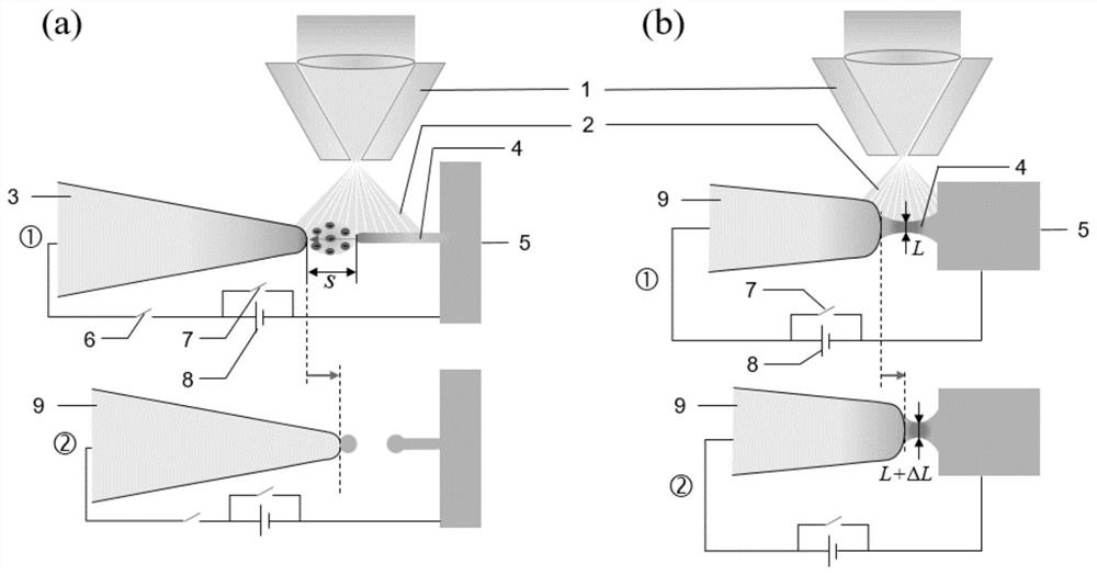
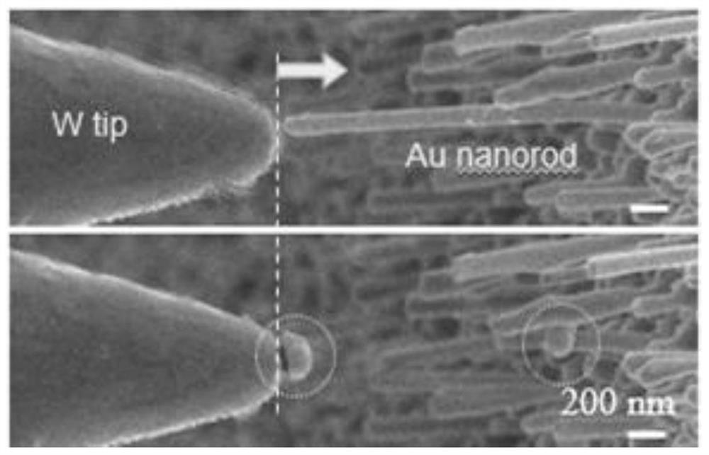
[0068] 1) Fix the Au substrate with Au nanocolumn arrays on the surface prepared by superplastic nano-casting on the sample stage of the scanning electron microscope, and fix a tungsten probe on a nano-manipulator installed in the scanning electron microscope. The manipulator has degrees of freedom in three directions and the movement accuracy can be better than 1 nanometer. First connect the tungsten needle tip to the Au substrate through a short-circuit through the output end of the nanomanipulator;

[0069] 2) When the electron beam of the scanning electron microscope is turned on (usually the acceleration voltage of the electron beam is set to be greater than or equal to 1 kV and less than or equal to 20 kV), the nanomanipulator is driven in situ to move, so that the tungsten tip approaches and touches an Au nanopillar , and then retract the tungsten probe to make it spaced from the Au nanocolumn at a certain distance (usually less than 2 microns), and simultaneously disconn...

Embodiment 2

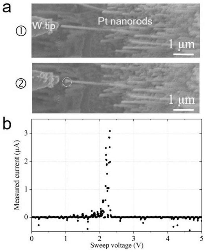
[0072] 1) Fix the Pt substrate with the Pt nanocolumn array on the surface prepared by superplastic nanomolding on the sample stage of the scanning electron microscope, and connect it to the tungsten tip installed on the nano manipulator through a wire short circuit;

[0073] 2) Drive the nanomanipulator to move in situ under the condition that the electron beam of the scanning electron microscope is turned on, so that the tungsten tip approaches and touches a Pt nanocolumn, and then retracts the tungsten probe so that it is separated from the Pt nanocolumn by a certain distance (usually less than 1 Micron), disconnect the wire between the tungsten tip and the Au substrate at the same time, and respectively connect the tungsten tip and the Pt substrate to the positive and negative poles of a voltage source, but the power supply of the voltage source is turned off;

[0074] 3) Drive the tungsten probe close to the Pt nanocolumn. During this process, the Pt nanocolumn is partiall...

Embodiment 3

[0078] The specific process steps for preparing a typical Pt-Ag nano-heterojunction device are as follows:

[0079] 1) Take the method steps of the aforementioned embodiments to first make a tungsten tip welded with a Pt nanocolumn;

[0080] 2) Replace the Pt sample on the SEM sample stage with an Ag substrate, and short-circuit the tungsten tip with the Pt nanocolumn welded to the Ag substrate;

[0081] 3) Drive the nanomanipulator to move in situ when the electron beam of the scanning electron microscope is turned on, so that the tungsten tip approaches and contacts an Ag nanopillar on the Ag substrate;

[0082] 4) Disconnect the short-circuit connection between the tungsten tip and the Ag substrate, apply a small voltage between the tungsten tip and the Ag substrate, and continuously increase the input voltage until welding occurs between the Pt nanocolumn and the Ag nanocolumn;

[0083] 5) Drive the tungsten tip to reciprocate and stretch and move laterally, so that the A...


PUM


Abstract

The invention discloses a method for cutting a metal nano structure to assemble the same into a nano device and a method of in-situ characterization for the nano device. The method for cutting and assembling the nano device is completed in situ under a scanning electron microscope, and comprises the following steps: (1) connecting a conductive probe with a metal nano structure through a wire in ashort-circuit manner, and controlling the conductive probe to be close to and in contact with the metal nano structure; (2) moving the conductive probe to enable the conductive probe to leave the metal nano structure, and disconnecting the short-circuit connection at the same time; and (3) moving the conductive probe to be close to the metal nano structure, so that the metal nano structure is locally melted and partially transferred and is attached to the tip of the conductive probe, so that a nano device with the metal nano structure attached to the tip and a metal nano structure with nanospheres formed at the tip of the metal nano structure are formed. A method of in situ characterization is also provided to obtain microstructure-electrical performance relationships. The method providedby the invention has a great reference value and application potential.

Description

technical field [0001] The invention belongs to the field of nano-manufacturing, and in particular relates to a method for cutting metal and metal alloy nanostructures, and a method for assembling and characterizing nano-devices. Background technique [0002] By modulating the shape of metal nanostructures, its optical, electrical, magnetic, and catalytic properties can be significantly improved, so it has a wide range of applications in batteries, catalysis, optics, sensing, and surface physical chemistry. Traditional methods of modulating the shape of metal nanostructures and fabricating devices based on metal nanostructures usually use advanced photolithography techniques. Since photolithography is based on a planar microfabrication process, there are still great challenges in the preparation of more complex three-dimensional nanostructures or nanodevices. Although focused ion beam technology can locally sculpt nanostructures, it is based on the bombardment of nanostruct...

Claims


Application Information

Patent Timeline
Patent Type & Authority Applications(China)
IPC IPC(8): B81C1/00B81B7/00B81B7/04B81C99/00
CPCB81C1/00015B81C1/00031B81C1/00007B81B7/00B81B7/04B81C99/0035
Inventor 刘泽
Owner WUHAN UNIV
Why Eureka
Try Eureka