A comprehensive recycling process for waste circuit board resources

A waste circuit board and process technology, which is applied in the field of high-efficiency and comprehensive recycling process of waste circuit boards, can solve the problems of cumbersome steps, long process and difficult control

Active Publication Date: 2021-05-14
CENT SOUTH UNIV
View PDF13 Cites 0 Cited by
  • Summary
  • Abstract
  • Description
  • Claims
  • Application Information

AI Technical Summary

Problems solved by technology

This method has a long process, cumbersome steps, and is difficult to control.

Method used


Image

  • A comprehensive recycling process for waste circuit board resources
  • A comprehensive recycling process for waste circuit board resources

Examples


Embodiment 1

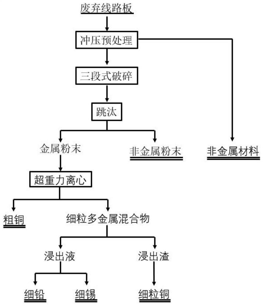
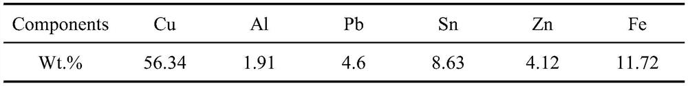
[0040] For waste circuit boards (the mass fraction of each component is shown in Table 1), carry out comprehensive recycling, including the following steps:

[0041] (1) Place the discarded circuit boards that have disassembled electronic components on a hydraulic punching machine for punching pretreatment, using a quantitative pump with a flow rate of 34.5 / min, a stroke of 180mm, and a punching time of 15n / min, and most of the low metal of copper and tin have been stripped The recovery rate of the non-metal part of the content is 16.7%;

[0042] (2) The remaining waste circuit boards are firstly crushed by a twin-shaft shearing crusher, and then screened. Materials with a particle size greater than 20mm continue to be returned to coarse crushing. Materials with a particle size of less than 0.6mm are collected for later use; materials with a particle size of 0.6-20mm Enter the hammer crusher for crushing, and then sieve. The material with a particle size greater than 1mm will ...

Embodiment 2

[0051] For waste circuit boards (the mass fraction of each component is shown in Table 1), carry out comprehensive recycling, including the following steps:

[0052] (1) Place the discarded circuit boards that have disassembled electronic components on a hydraulic punching machine for punching pretreatment. A quantitative pump with a flow rate of 49.5L / min is used, the stroke is 250mm, and the punching time is 20n / min. Most of the copper and tin have been stripped. The recovery rate of non-metallic materials with metal content is 19.2%;

[0053] (2) The remaining waste circuit boards are firstly crushed by a twin-shaft shearing crusher, and then screened. Materials with a particle size greater than 25mm continue to be returned to coarse crushing. Materials with a particle size of less than 0.6mm are collected for later use; materials with a particle size of 0.6-25mm Enter the hammer crusher for crushing, and then sieve, the material with a particle size greater than 2mm will c...


PUM


Abstract

A comprehensive recycling process for waste circuit board resources, comprising the following steps: (1) performing stamping pretreatment on waste circuit boards that have disassembled electronic components, so that multilayer composite materials are initially dissociated and non-metallic materials are recovered; (2) After three-stage crushing of the remaining waste circuit boards, jigging separation is carried out to obtain non-metallic powder and metal powder; (3) separation of metal powder to obtain crude copper and fine-grained polymetallic mixture; (4) fine-grained polymetallic mixture Alkali leaching, solid-liquid separation to obtain lead and tin-containing leaching solution and copper-containing leaching slag, adding sodium sulfide precipitant to the lead and tin-containing leaching solution, solid-liquid separation to obtain lead-containing precipitation and tin-containing solution, and the tin-containing solution is spun After the galvanic deposition recovers tin, it returns to the alkaline leaching process, and the copper-containing leaching slag recovers fine-grained copper. The invention realizes full resource recovery of waste circuit boards, has the advantages of high recovery efficiency, no pollution, simple operation, etc., and is suitable for large-scale recovery of waste circuit boards in industry.

Description

technical field [0001] The invention discloses a high-efficiency comprehensive recovery process for waste circuit boards, and relates to the field of waste resource recovery. Background technique [0002] In recent years, the development of my country's electronic information industry has continuously made new achievements. In 2018, the revenue scale of the electronics manufacturing industry was 10.6 trillion yuan, an increase of 9.0%, which was 3.4 percentage points higher than the industrial average. Among them, the production of the electronic device industry grew steadily and rapidly, and the printed circuit industry As the carrier of electronic devices, boards are widely used in high-tech fields such as military industry, medical treatment, communication, smart phones, and industrial control, and their manufacturing industry has also developed rapidly. Since 2006, China has surpassed Japan to become the world's largest and fastest-growing printed circuit board manufactur...

Claims


Application Information

Patent Timeline
Patent Type & Authority Patents(China)
IPC IPC(8): B09B3/00B03B5/10B04B13/00C22B7/00C22B15/00C22B13/00C22B25/06
CPCB03B5/10B04B13/00C22B7/008C22B13/045C22B15/0065C22B15/0089C22B25/04C22B25/06Y02W30/82Y02P10/20
Inventor 孙伟曹杨唐鸿鹄杨越李梦闪
Owner CENT SOUTH UNIV
Why Eureka
Try Eureka