A kind of preparation method based on surface pn crystalline silicon solar cell
A technology of silicon solar cells and crystals, applied in the field of solar photovoltaics, can solve the problems of low accuracy, inability to meet accurate, fast measurement of solar radiation, slow response, etc., to achieve the effect of improving conversion efficiency, reducing dead layers, and increasing Voc
- Summary
- Abstract
- Description
- Claims
- Application Information
AI Technical Summary
Problems solved by technology
Method used
Image
Examples
Embodiment 1
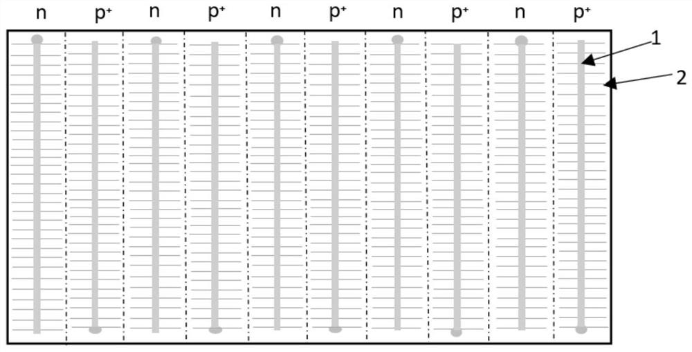
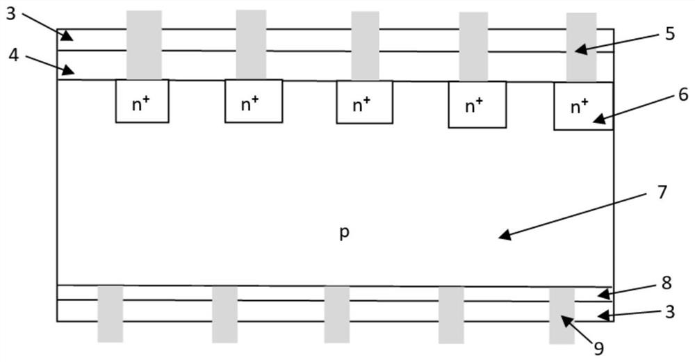
[0039] Referring to Figure 4(a), a surface n + The preparation method of the p-crystalline silicon solar cell is as follows: first, a p-type silicon wafer 7 with a resistivity of 2Ω·cm and a thickness of 400um is selected, the surface of the p-type silicon wafer 7 is ultrasonically cleaned with an electronic cleaning agent, and then the surface of the p-type silicon wafer 7 is cleaned by mass percentage concentration. 1.5%, the temperature is 82 ℃ of sodium hydroxide solution to corrode the texturing, the texturing time is 20min, after the texture preparation is completed, the silicon wafer is sprayed, pickled, rinsed, pre-dehydrated and dried.
[0040] Then, the surface of the silicon wafer after texturing is oxidized to form a silicon dioxide film, wherein the oxidation temperature is 850° C. and the oxidation time is 30 minutes to form a silicon dioxide film with a thickness of about 0.3um.
[0041] For photolithography of the oxidized silicon wafer, first, spin-coat the po...
Embodiment 2
[0056] Referring to Fig. 4(b), a surface p + The preparation method of the n-crystalline silicon solar cell is as follows: first, an n-type silicon wafer 11 with a resistivity of 2Ω·cm and a thickness of 400um is selected, and the surface of the n-type silicon wafer 11 is ultrasonically cleaned with an electronic cleaning agent. 1.5%, the temperature is 82 ℃ of sodium hydroxide solution to corrode the texturing, the texturing time is 15min, after the preparation is completed, the silicon wafer is sprayed, pickled, rinsed, pre-dehydrated and dried.
[0057] Then, the surface of the silicon wafer after texturing is oxidized to form a silicon dioxide film, wherein the oxidation temperature is 850° C., and the oxidation time is 40 minutes to form a silicon dioxide film with a thickness of about 0.35um.
[0058] For photolithography of the oxidized silicon wafer, first, spin-coat the positive photoresist evenly on the silicon wafer by spin coating. The spin coating speed is 2000rpm...
Embodiment 3
[0073] Referring to Figure 4(a), a surface n + The preparation method of p-crystalline silicon solar cell is as follows: first, select a p-type original silicon wafer with a resistivity of 1Ω·cm and a thickness of 100um, use an electronic cleaning agent to ultrasonically clean the surface of the original silicon wafer, and then use a mass percentage concentration of 1%. , the temperature is 80 ℃ sodium hydroxide solution for etching and texturing, and the texturing time is 15min. After the preparation is completed, the silicon wafers are sprayed, pickled, rinsed, pre-dehydrated and dried.
[0074] Then, the surface of the silicon wafer after texturing is oxidized to form a silicon dioxide film, wherein the oxidation temperature is 1000° C., and the oxidation time is 10 minutes to form a silicon dioxide film with a thickness of about 0.2um.
[0075] For photolithography of the oxidized silicon wafer, first, spin-coating the positive photoresist uniformly on the silicon wafer, t...
PUM
| Property | Measurement | Unit |
|---|---|---|
| thickness | aaaaa | aaaaa |
| thickness | aaaaa | aaaaa |
| thickness | aaaaa | aaaaa |
Abstract
Description
Claims
Application Information
 - R&D
- Intellectual Property
- Life Sciences
- Materials
- Tech Scout
- Unparalleled Data Quality
- Higher Quality Content
- 60% Fewer Hallucinations
Browse by: Latest US Patents, China's latest patents, Technical Efficacy Thesaurus, Application Domain, Technology Topic, Popular Technical Reports.
© 2025 PatSnap. All rights reserved.Legal|Privacy policy|Modern Slavery Act Transparency Statement|Sitemap|About US| Contact US: help@patsnap.com


