High-performance MIS gate enhanced GaN-based high-electron-mobility transistor and preparation method thereof

A high-electron mobility, high-performance technology, applied in semiconductor/solid-state device manufacturing, circuits, electrical components, etc., can solve the problems of insufficient bearing reverse withstand voltage, uneven current concentration, buffer layer current leakage, etc. , to ensure high electron mobility, smooth electron transport, and reduce reverse leakage current.

Active Publication Date: 2020-09-18
SOUTH CHINA NORMAL UNIVERSITY
View PDF7 Cites 3 Cited by
  • Summary
  • Abstract
  • Description
  • Claims
  • Application Information

AI Technical Summary

Problems solved by technology

[0005] Although the groove gate MIS structure HEMT has higher current density and lower on-resistance, due to the potential difference between its source-gate and drain-gate, the electric field is crowded on the side close to the drain, causing the buffer layer current to leak, It is easy to cause ionization impact to generate an avalanche process, resulting in device breakdown
At the same time, there are more electronic well states between the dielectric layer and the AlGaN barrier layer, which makes the current concentration under the gate from the source to the drain uneven, and the AlGaN barrier layer does not actually fully play the role of reverse withstand voltage. The role of the device, resulting in the breakdown voltage of the device is often lower than the theoretical expected value

Method used


Image

  • High-performance MIS gate enhanced GaN-based high-electron-mobility transistor and preparation method thereof
  • High-performance MIS gate enhanced GaN-based high-electron-mobility transistor and preparation method thereof

Examples


Embodiment Construction

[0044] Next, the technical solutions in the embodiments of the present invention will be clearly and completely described in conjunction with the accompanying drawings of the present invention, and the described embodiments are only some of the embodiments of the present invention, not all of them. Based on the embodiments of the present invention, other embodiments obtained by persons of ordinary skill in the art without making creative efforts all belong to the protection scope of the present invention.

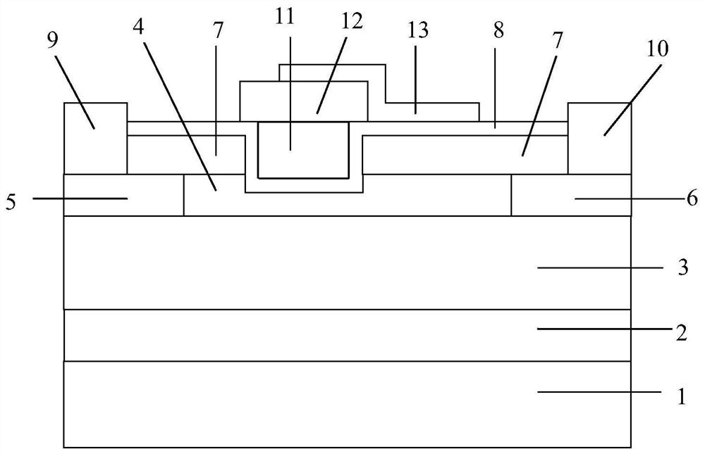
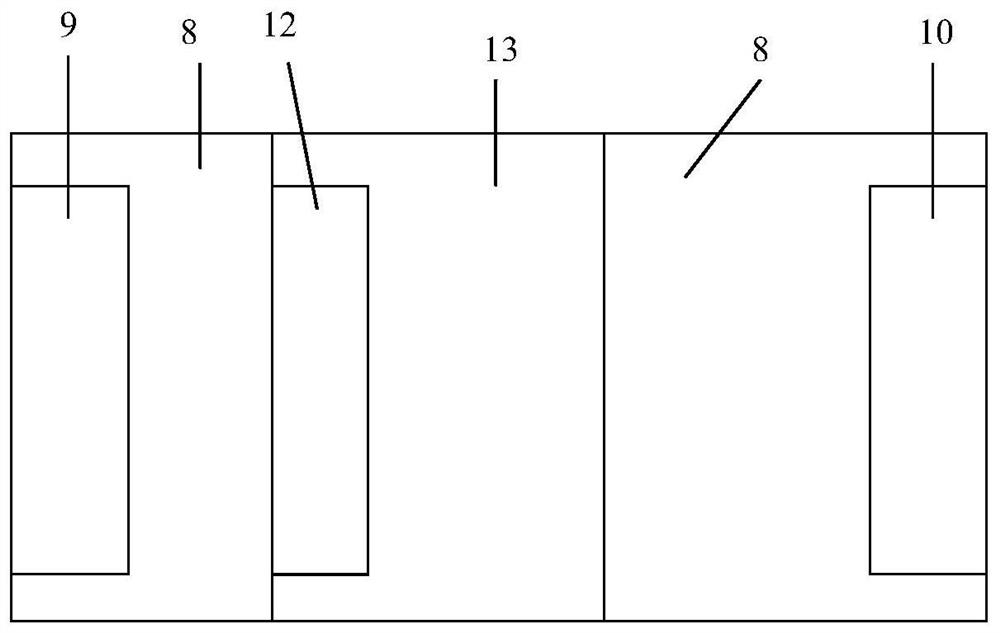
[0045] The present invention will be described in further detail below. Such as Figure 1-2 As shown, the present invention provides a high-performance MIS gate-enhanced GaN-based high electron mobility transistor, which includes a silicon substrate 1, an AlN nucleation layer 2, a GaN buffer layer 3, and an AlGaN layer stacked in sequence. The AlGaN layer consists of an AlGaN barrier layer 4 , a p-doped drift AlGaN region 5 and an n-doped drift AlGaN region 6 .

[0046]A ...


PUM

PropertyMeasurementUnit
thicknessaaaaaaaaaa
thicknessaaaaaaaaaa
thicknessaaaaaaaaaa

Abstract

The invention relates to a high-performance MIS gate enhanced GaN-based high-electron-mobility transistor and a preparation method thereof. The device comprises an AlGaN layer which is positioned on asubstrate, and the AlGaN layer is composed of an AlGaN barrier layer, a p-doped drift region and an n-doped drift region, wherein the p-doped drift region and the n-doped drift region are distributedon the two sides of the AlGaN barrier layer, the passivation layer is located between the source electrode and the drain electrode, and the groove extends into the barrier layer from the passivationlayer and fills the p-GaN region of the groove, the grid electrode located on the p-GaN region and the field plate. According to the invention, n / p doped layers with different gradients are formed onthe two sides of the barrier layer, and the current crowding in the source-drain direction is suppressed; meanwhile, p-GaN is connected below the grid electrode, the upper portion of the grid electrode makes contact with the field plate, charge congestion below the grid electrode is controlled, electron transport of the two-dimensional electron gas channel is smoother, and under the condition thathigh current density and high electron mobility of the device are guaranteed, adjustable and controllable improvement of breakdown voltage is achieved, on-resistance is reduced, and power characteristics and reliability of the device are improved.

Description

technical field [0001] The invention relates to the field of high electron mobility transistors, in particular to a high-performance MIS gate enhanced GaN-based high electron mobility transistor and a preparation method thereof. Background technique [0002] With the development of clean energy, automation equipment, communication technology, automotive electronics, and switching power supplies, the performance of power semiconductor devices has attracted much attention. As a representative of the third-generation semiconductor materials, GaN-based materials are often used in the production of high-temperature, high-frequency and high power electronics. In addition, the modulated doped AlGaN / GaN heterostructure has better electron mobility, saturated electron velocity and higher two-dimensional electron gas density than GaN materials and second-generation semiconductor materials at room temperature. It is an ideal material for power devices, so AlGaN / GaN heterojunction hig...

Claims


Application Information

Patent Timeline
Patent Type & Authority Applications(China)
IPC IPC(8): H01L29/778H01L29/06H01L29/40H01L21/335
CPCH01L29/7786H01L29/0607H01L29/0684H01L29/402H01L29/66462
Inventor 郭志友李渊夏凡谭秀洋马建铖夏晓宇张淼
Owner SOUTH CHINA NORMAL UNIVERSITY
Why Eureka
Try Eureka