Device for read-write control based on time division multiplexing in DDR3

A technology of time-division multiplexing and write control, which is applied in the direction of instrumentation, electrical digital data processing, etc., to achieve the effects of simple structure, improved system operating frequency, and reduced implementation cost

Pending Publication Date: 2020-09-22
UNIV OF ELECTRONICS SCI & TECH OF CHINA
View PDF4 Cites 4 Cited by
  • Summary
  • Abstract
  • Description
  • Claims
  • Application Information

AI Technical Summary

Problems solved by technology

[0003] Due to the improvement of technical requirements, it is often necessary to process multiple signal data on one chip in some hardware implementations. For example, for a wireless communication system that needs to support multi-user access and support multiple information rates, its baseband processing needs to be processed in FPGA In order to improve the resource consumption problem caused by multi-channel signals, DDR3 will be considered to store the intermediate processed data at this time, but based on the consideration of cost and DDR3 storage characteristics, when it is necessary to process multiple independent signals, DDR Only one signal can be supported for reading or writing at the same time

Method used


Image

  • Device for read-write control based on time division multiplexing in DDR3
  • Device for read-write control based on time division multiplexing in DDR3
  • Device for read-write control based on time division multiplexing in DDR3

Examples


example 1

[0037] Example 1: FPGA simulation and implementation of matrix interleaving of multiple independent signals using DDR3

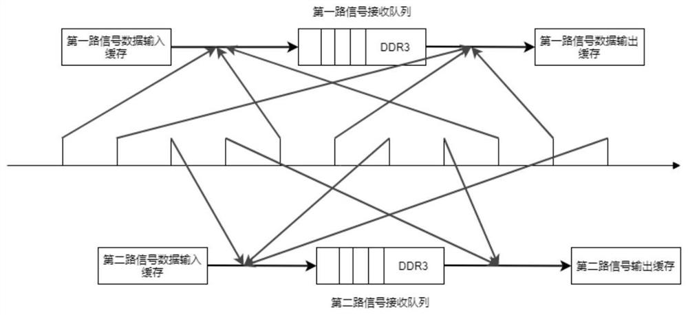
[0038] The simulation platform used in Example 1 is Matlab, Vivado 2018.2 and Modelsim 10.6e, and the implemented architecture is as follows Figure 4 As shown, the implemented function is based on the time-division multiplexing technology proposed in this paper, and the matrix column permutation and interleaving process of two independent signals is completed in one piece of DDR3. First in Matlab based on Figure 4 Establish a simulation platform for matrix interleaving and deinterleaving in the data conversion process: generate data sources, and simulate on the simulation platform to obtain the output data of each module and the final correct simulation results, which are used for comparison with FPGA simulation and implementation results.

[0039] exist Figure 4 The input data in is the same source data used by the Matlab simulation platform. In the da...

example 2

[0042] Example 2: Example 1 implements the analysis of throughput and DDR3 speed in the model

[0043] The simulation platform used in Example 2 is Vivado 2018.2 and Modelsim 10.6e. In the example, the working frequency of DDR3 is 400MHZ, the data bit width is 16bit, and the working mode of burst length is 8. The data throughput rate input by the data combination module is 0.85Gb / s, and the speed that DDR3 writes data can reach is 1.02Gb / s. The DDR3 write data rate is greater than the input data throughput rate, and the process of writing data can be completed correctly. Similarly, the read data throughput rate of the decompression module is 1.19Gb / s, and the DDR3 read data rate is 1.13Gb / s. The DDR3 read data rate is lower than the throughput rate of the dedata module output data, and the data read process can be completed correctly.

[0044] Since the interleaving principle involves the sequence conversion of data, the write address sequence of the DDR3 data writing process...


PUM


Abstract

In order to solve the problem that read-write control of a DDR3 over different signals needs to be reasonably achieved in order to achieve data storage and conversion of multiple paths of independentsignals on one DDR3, the invention provides a device for read-write control based on time division multiplexing in DDR3. The device comprises a time division multiplexing module, a DDR3 write controlstate machine module, a DDR3 read control state machine module, a DDR3 read-write data module, a DDR3 read-write address module and a read-write command signal generation module. The time division multiplexing module is used for generating exclusive read time slots and write time slots of independent signals, and the read and write processes of the paths of signals are completely independent; theDDR3 read and write control state machine modules are used for controlling the data reading and writing processes of the DDR3 respectively; and the DDR3 read-write data, address and read-write commandsignal generation modules are used for completing the most direct data interaction process with the DDR3. The hardware implementation structure is simple, flexible and configurable, the implementation cost can be reduced, and the system operation frequency can be improved under certain conditions.

Description

technical field [0001] The invention relates to the read-write control technology of DDR3 memory, in particular to the technology of time-division multiplexing read-write control in DDR3. Background technique [0002] The improvement of human needs in various aspects has promoted the development of science and technology. As the double-rate synchronous dynamic memory DDR SDRAM (Double Data Rate Synchronous Dynamic Random Access Memory), which is widely used in memory, it has also developed rapidly. Due to the high speed of DDR3, low power consumption, low heat generation and relatively low cost, DDR3 is currently widely used on FPGA development boards. The use of DDR3 in FPGA implementation, on the one hand, is to store large-capacity data to reduce the consumption of storage resources in the FPGA chip; the other is to use the high speed of DDR3 to improve the data throughput rate of the system and reduce processing delay time. In addition, DDR3 can also conveniently transf...

Claims


Application Information

Patent Timeline
Patent Type & Authority Applications(China)
IPC IPC(8): G06F13/16
CPCG06F13/1689G06F13/1668
Inventor 何春任跃李小林程郁凡
Owner UNIV OF ELECTRONICS SCI & TECH OF CHINA
Why Eureka
Try Eureka