
GaN-based laser diode epitaxial structure and preparation method thereof

A laser diode and epitaxial structure technology, applied in the structure of optical waveguide semiconductors, lasers, laser parts, etc., can solve the problems of high beam quality, narrow half-peak width, low beam quality, etc., and achieve the effect of high beam quality

Active Publication Date: 2020-09-22
DONGGUAN UNIV OF TECH
View PDF12 Cites 4 Cited by
  • Summary
  • Abstract
  • Description
  • Claims
  • Application Information

AI Technical Summary

Problems solved by technology

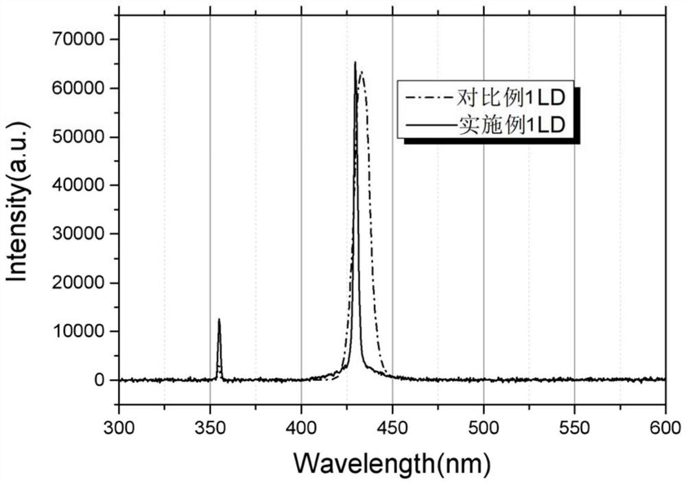
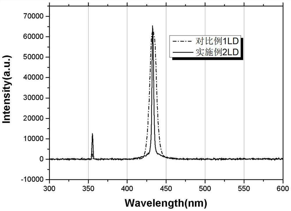
[0006] In order to overcome the defects of low beam quality described in the prior art, the present invention provides a gallium nitride-based laser diode epitaxial structure, the provided gallium nitride-based laser diode epitaxial structure is used as a laser, and when optically pumped , the half maximum width is narrow, and the beam quality is high

Method used


Image

  • GaN-based laser diode epitaxial structure and preparation method thereof
  • GaN-based laser diode epitaxial structure and preparation method thereof
  • GaN-based laser diode epitaxial structure and preparation method thereof

Examples


Embodiment 1

[0043] This embodiment provides a GaN-based laser diode epitaxial structure, such as figure 1 As shown, a gallium nitride single crystal substrate 101, an n-type GaN layer 102, an n-type confinement layer 103, a lower waveguide layer 104, an active region 105, an upper waveguide layer 106, and a p-type confinement layer are sequentially stacked from bottom to top. layer 107 and p-type GaN layer 108.

[0044] The preparation method and specific parameters of the GaN-based laser diode epitaxial structure are as follows:

[0045] S1. First in the metal organic compound vapor phase epitaxy reaction chamber, in hydrogen (H 2 ) atmosphere, the temperature was raised to 500°C, and NH was introduced into the reaction chamber 3 , and then heated to 1050°C, under hydrogen (H 2 ) and ammonia (NH 3 ) under a mixed atmosphere at a temperature of 1050° C., the surface of the GaN substrate is activated for 5 minutes.

[0046] S2. In hydrogen (H 2 ) atmosphere, on a GaN substrate, at a ...

Embodiment 2

[0066] This embodiment provides a GaN-based laser diode epitaxial structure, such as figure 1 As shown, a gallium nitride single crystal substrate 101, an n-type GaN layer 102, an n-type confinement layer 103, a lower waveguide layer 104, an active region 105, an upper waveguide layer 106, and a p-type confinement layer are sequentially stacked from bottom to top. layer 107 and p-type GaN layer 108.

[0067] The preparation method and specific parameters of the GaN-based laser diode epitaxial structure are as follows:

[0068] S1. First in the metal organic compound vapor phase epitaxy reaction chamber, in hydrogen (H 2 ) atmosphere, the temperature was raised to 500°C, and NH was introduced into the reaction chamber 3 , and then heated to 1050°C, under hydrogen (H 2 ) and ammonia (NH 3 ) under a mixed atmosphere at a temperature of 1050° C., the surface of the GaN substrate is activated for 5 minutes.

[0069] S2. In hydrogen (H 2 ) atmosphere, on a GaN substrate, at a ...


PUM

PropertyMeasurementUnit
Thicknessaaaaaaaaaa
Thicknessaaaaaaaaaa
Thicknessaaaaaaaaaa

Abstract

The invention discloses a GaN-based laser diode epitaxial structure and a preparation method thereof. The GaN-based laser diode epitaxial structure is sequentially provided with a GaN single crystal substrate, an n-type GaN layer, an n-type limiting layer, a lower waveguide layer, an active region, an upper waveguide layer, a p-type limiting layer and a p-type GaN layer from bottom to top in a stacked mode, wherein the lower waveguide layer is an n<->-Aly2Ga<1-y2>N+n<->-GaN+n<->Inx1Ga<1-x1>N / GaN superlattice composite waveguide layer; the active region is of an asymmetrically doped InGaN / GaN double quantum well structure, and the upper waveguide layer is of a u<->Inx4Ga<1-x4>N / GaN superlattice and u<->GaN+p<->Aly4Ga<1-y4>N composite structure. The brand-new GaN-based laser diode epitaxialstructure is obtained by optimally designing a GaN-based laser high-quantum-efficiency gradient In component trapezoidal active region structure and further designing a novel optical waveguide layer structure. The GaN-based laser diode epitaxial structure is used as a laser, and when optical pump lasing is carried out, the half-peak width is narrow, and the light beam quality is high.

Description

technical field [0001] The invention relates to the technical field of laser diodes, in particular to a GaN-based laser diode epitaxial structure and a preparation method thereof. Background technique [0002] Group III-V nitride semiconductor materials are the third-generation semiconductor materials after silicon and gallium arsenide, including gallium nitride (GaN), aluminum nitride (AlN), indium nitride (InN) and their alloys , is a direct bandgap semiconductor, which has the advantages of large band gap (range 0.7-6.2eV), high breakdown electric field, high thermal conductivity, high electron saturation rate, strong radiation resistance and chemical corrosion resistance. These advantages in optoelectronic properties make III-V nitride materials have a strong competitive advantage in the field of optoelectronics (such as LED and LD), and are in an irreplaceable position. It is an ideal material for making semiconductor lasers from ultraviolet to green light bands. [0...

Claims


Application Information

Patent Timeline
IPC IPC(8): H01S5/343H01S5/20
CPCH01S5/20H01S5/34333H01S5/34346
Inventor 贾传宇
Owner DONGGUAN UNIV OF TECH
Learn More