
A kind of preparation method of silicon-based wide-spectrum photodetector

A photodetector and wide-spectrum technology, applied in circuits, electrical components, semiconductor devices, etc., can solve the problems of low detection efficiency, achieve high detection efficiency and improve device efficiency

Active Publication Date: 2022-07-22
SHANGHAI INST OF MICROSYSTEM & INFORMATION TECH CHINESE ACAD OF SCI
View PDF0 Cites 1 Cited by
  • Summary
  • Abstract
  • Description
  • Claims
  • Application Information

AI Technical Summary

Problems solved by technology

[0005] The technical problem to be solved by the present invention is to provide a method for preparing a silicon-based wide-spectrum photodetector to overcome the defects of low detection efficiency of photodetectors from visible light to infrared light in the prior art

Method used


Image

  • A kind of preparation method of silicon-based wide-spectrum photodetector
  • A kind of preparation method of silicon-based wide-spectrum photodetector
  • A kind of preparation method of silicon-based wide-spectrum photodetector

Examples


Embodiment 1

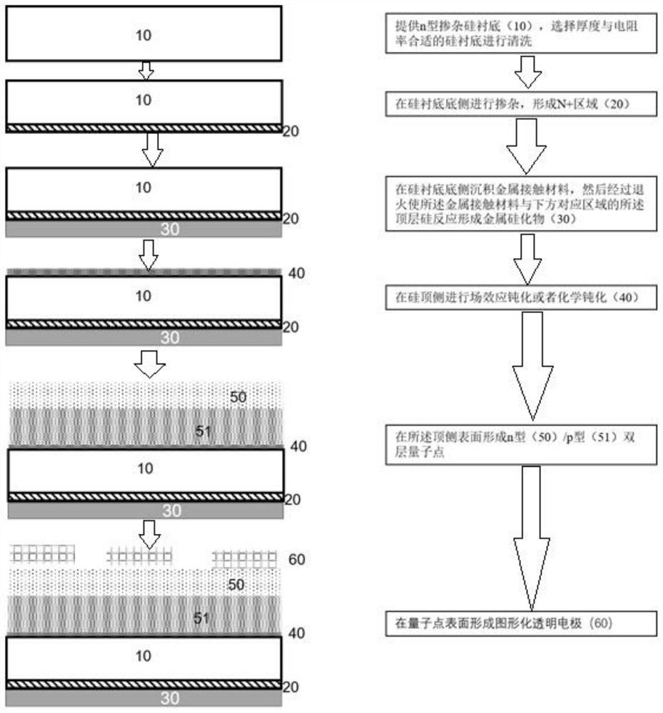
[0049] The present embodiment provides a preparation method of a silicon-based wide-spectrum photodetector, and the specific steps are as follows:

[0050] (1) Provide an n-type doped silicon substrate, which is a P-doped semiconductor (Si), 100 crystal planes, selected thickness of 0.5 mm, and resistivity of 1-10 Ω.cm; Standard RCA process cleaning and 1:20 (HF:H 2 Rinse with HF solution in a volume ratio of O=1:20 to remove the natural oxide layer;

[0051] (2) Doping P ions on the bottom side of the silicon substrate with a doping concentration of 5×10 15 cm -2 , the doping energy is 20keV, the N+ region is formed and the lattice damage is eliminated by annealing at 1000℃ for 5s (need to be carried out under the protection of vacuum environment or inert atmosphere);

[0052] (3) in N + The metal contact material Al is deposited on the bottom side of the region by electron beam evaporation, with a thickness of 100 nm, and then annealed at 400 ° C (need to be carried out ...

Embodiment 2

[0059] (1) Provide an n-type doped silicon substrate, the substrate includes, P-doped Si, 100 crystal plane, the selected thickness is 0.5mm, and the resistivity is 1-10Ω.cm; standard RCA is performed for a suitable silicon substrate Process cleaned and washed with 1:20 (HF:H 2 Rinse with HF solution in a volume ratio of O=1:20 to remove the natural oxide layer;

[0060] (2) Growth of barrier layer SiO by CVD method on the front side of silicon substrate 2 , its thickness is 500nm;

[0061] (3) Diffusion the silicon wafer, the diffusion temperature is 700°C, the diffusion time is 5min, and the diffusion furnace needs to be protected with an inert gas;

[0062] (4) Use 1:10 (HF:H 2 O=1:10 volume ratio) HF solution will SiO 2 Rinse off, the processing time is about 10 minutes;

[0063] (3) in N + The bottom side of the region is deposited by electron beam evaporation, the metal contact material Al, with a thickness of 100nm, is then annealed at 400 °C under the protection ...

Embodiment 3

[0068] (1) Provide an n-type doped silicon substrate, the substrate includes, P-doped Si, 100 crystal plane, the selected thickness is 0.5mm, and the resistivity is 1-10Ω.cm; standard RCA is performed for a suitable silicon substrate Process cleaned and washed with 1:20 (HF:H 2 Rinse with HF solution in a volume ratio of O=1:20 to remove the natural oxide layer;

[0069] (2) Doping P ions on the bottom side of the silicon substrate with a doping concentration of 5×10 15 cm -2 , the doping energy is 20keV, the N+ region is formed and the lattice damage is eliminated by annealing at 1000℃ for 5s under the protection of vacuum environment or inert atmosphere;

[0070] (3) in N + The bottom side of the region is deposited by electron beam evaporation, the metal contact material Al, with a thickness of 100nm, is then annealed at 400 °C under the protection of a vacuum environment or an inert atmosphere for 30s, and the metal silicon is reacted on the silicon surface to form meta...


PUM

PropertyMeasurementUnit
thicknessaaaaaaaaaa
thicknessaaaaaaaaaa
thicknessaaaaaaaaaa

Abstract

The invention relates to a preparation method of a silicon-based wide-spectrum photodetector, comprising: cleaning an n-type doped silicon substrate; doping on the bottom side of the n-type doped silicon substrate to form N + area; in the N + Metal contact material is deposited on the bottom side of the region, and then annealed to make the metal contact material react with the top layer silicon in the corresponding region to form metal silicide; passivation is performed on the top side of the n-type doped silicon substrate to form passivation layer; forming n-type / p-type double-layer quantum dots on the surface of the passivation layer; forming a patterned transparent electrode on the surface of the quantum dots. The detector prepared by the method has high detection efficiency from visible light to infrared light, is compatible with Si-based CMOS integrated circuits, and does not pollute the substrate.

Description

technical field [0001] The invention belongs to the field of photodetector preparation, in particular to a preparation method of a silicon-based wide-spectrum photodetector. Background technique [0002] Infrared detection has better adaptability to the environment than visible light, and can work at night and in harsh environments. Infrared detection has good concealment, is safer than radar and laser detection, and has a higher recognition rate for camouflaged targets. Compared with radar systems, infrared systems have the advantages of small size, light weight, and low power consumption. Therefore, infrared detection in the military can be applied to infrared night vision, infrared guidance, and infrared reconnaissance. Infrared detection technology not only has many applications in the military field, after the transformation and process improvement of advanced research results in the military field, infrared detectors have also been widely used in the civilian field. In...

Claims


Application Information

Patent Timeline
Patent Type & Authority Patents(China)
IPC IPC(8): H01L31/0352H01L31/09H01L31/18
CPCH01L31/1804H01L31/186H01L31/1868H01L31/1864H01L31/1884H01L31/035218H01L31/09H01L31/1812Y02P70/50
Inventor 郑理周文程新红俞跃辉
Owner SHANGHAI INST OF MICROSYSTEM & INFORMATION TECH CHINESE ACAD OF SCI
Learn More