Device and method for preparing silicon dioxide and polycrystalline silicon films on surface of silicon wafer

A technology of polysilicon thin film and silicon dioxide, which is applied in the fields of final product manufacturing, sustainable manufacturing/processing, electrical components, etc., can solve problems such as high cost, impact on industrial development, immature polysilicon film technology, etc., and achieve low cost, The effect of cheap target material and simple structure

Pending Publication Date: 2020-10-02
普乐(合肥)光技术有限公司
View PDF0 Cites 0 Cited by
  • Summary
  • Abstract
  • Description
  • Claims
  • Application Information

AI Technical Summary

Problems solved by technology

[0007] However, in the prior art, dense SiO is prepared on the surface of the silicon wafer 2 The technology of the film layer and a layer of highly doped polysilicon film layer is immature and the cost is high, which affects the development of the industry

Method used


Image

  • Device and method for preparing silicon dioxide and polycrystalline silicon films on surface of silicon wafer
  • Device and method for preparing silicon dioxide and polycrystalline silicon films on surface of silicon wafer

Examples


Embodiment 1

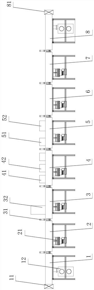
[0036] see figure 1 , a device for preparing silicon dioxide and polysilicon films on the surface of a silicon wafer, including an inlet pre-pumping chamber 1, an inlet transition chamber 2, an oxidation chamber 3, a process chamber 4, a tempering chamber 5, a cooling chamber 6, The outlet buffer chamber 7, the outlet chamber 8, and the connection between any two adjacent chambers are provided with a vacuum isolation flapper valve 31, and the front side of the inlet pre-pumping chamber 1 is provided with a first flap valve 11 , the rear side of the outlet chamber 8 is provided with a second flap valve 81, the inlet pre-pumping chamber 1 and the outlet chamber 8 are connected with a vacuum pump 12, the inlet transition chamber 2, the oxidation chamber 3, the process chamber 4 , the tempering chamber 5, the cooling chamber 6, and the outlet buffer chamber 7 are all connected with a turbomolecular pump 21, and the oxidation chamber 3 is connected with a low-energy oxygen ion sour...

Embodiment 2

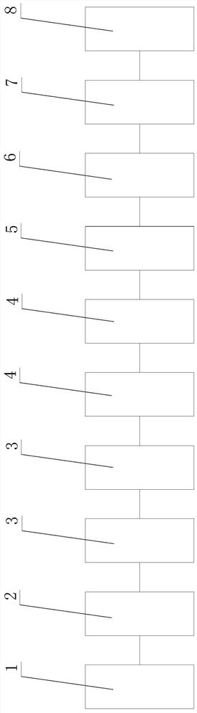
[0040] see figure 2 , a device for preparing silicon dioxide and polysilicon films on the surface of a silicon wafer, including an inlet pre-pumping chamber 1, an inlet transition chamber 2, two oxidation chambers 3, two process chambers 4, a tempering chamber 5, The cooling chamber 6, the outlet buffer chamber 7, the outlet chamber 8, and the connection between any two adjacent chambers are provided with a vacuum isolation plug valve 31, and the front side of the inlet pre-pumping chamber 1 is provided with a first The flap valve 11, the rear side of the outlet chamber 8 is provided with a second flap valve 81, the inlet pre-pumping chamber 1 and the outlet chamber 8 are connected with a vacuum pump 12, the inlet transition chamber 2, the oxidation chamber 3 , the process chamber 4, the tempering chamber 5, the cooling chamber 6, and the outlet buffer chamber 7 are all connected with a turbomolecular pump 21, and the oxidation chamber 3 is connected with a low-energy oxygen ...

Embodiment 3

[0044] Prepare the preparation method of silicon dioxide and polysilicon thin film on the surface of silicon chip, comprise the following steps:

[0045] (1) arrange the silicon wafers in a determinant on the graphite tray;

[0046] (2) Open the first flap valve, the graphite tray loaded with silicon wafers first enters the inlet pre-pumping chamber, and the air pressure is reduced from normal pressure to 1pa under the action of the vacuum pump;

[0047] (3) Open the vacuum isolation plug valve between the inlet pre-pumping chamber and the inlet transition chamber to send the graphite tray loaded with silicon wafers into the inlet transition chamber, and then close the vacuum isolation plug between the inlet pre-pumping chamber and the inlet transition chamber The plate valve, under the action of the turbomolecular pump, reduces the air pressure to 10 -2 pa;

[0048] (4) Open the vacuum isolation slide valve between the inlet transition chamber and the oxidation chamber to s...


PUM

PropertyMeasurementUnit
thicknessaaaaaaaaaa
thicknessaaaaaaaaaa
thicknessaaaaaaaaaa

Abstract

The invention discloses a device for preparing a silicon dioxide film and a polycrystalline silicon film on the surface of a silicon wafer. The device comprises an inlet pre-pumping chamber, an inlettransition chamber, at least one oxidation chamber, at least one process chamber, a tempering chamber, a cooling chamber, an outlet buffer chamber and an outlet chamber which are sequentially connected in series from front to back, wherein a vacuum isolation gate valve is arranged at the joint of any two adjacent chambers, flap valves are respectively arranged in the inlet pre-pumping chamber andthe outlet chamber, the inlet pre-pumping chamber and the outlet chamber are connected with a vacuum pump, the inlet transition chamber, the oxidation chamber, the process chamber, the tempering chamber, the cooling chamber and the outlet buffer chamber are connected with turbo molecular pumps, the oxidation chamber is connected with a low-energy oxygen ion source, a silicon target and a gaseous doping source are arranged in the working chamber, an infrared heating source is arranged at the front portion in the tempering chamber, and an ultraviolet laser tempering system is arranged at the rear portion in the tempering chamber. According to the invention, when the device is used, silicon wafers are placed on a graphite tray and sequentially react through the chambers, and the device is simple in structure, low in manufacturing cost and low in cost in the using process.

Description

technical field [0001] The invention relates to a device and a preparation method for preparing silicon dioxide and polysilicon thin films on the surface of a silicon chip. Background technique [0002] At present, grid parity requires the development of the photovoltaic industry to focus on higher photoelectric conversion efficiency. Existing high-efficiency crystalline silicon solar cell technology routes: P-PERC (Passivated Emitter and Rear Cell, passivated emitter back field point contact), N-PERT (Passivated Emitter Rear Totally-diffused cell, passivated emitter rear surface fully diffused ), HJT (Heterojunction, heterojunction), IBC (Inter-digitated back-contact, insert finger back junction back contact), MWT (Metal Wrap Through, metal perforation winding); TOPCon (Tunnel Oxide PassivatedContact, tunnel oxide passivated contact chemical contact). [0003] P-PERC cells limit the contact range on the back to the opening area, which increases the complexity of the proce...

Claims


Application Information

Patent Timeline
Patent Type & Authority Applications(China)
IPC IPC(8): H01L31/18H01L31/0216H01L31/0236
CPCH01L31/02168H01L31/0236H01L31/1864H01L31/1872H01L31/1876Y02P70/50
Inventor 孙巍泉
Owner 普乐(合肥)光技术有限公司
Why Eureka
Try Eureka