

Magnetic random access memory and forming method thereof
A random access memory and magnetic storage technology, applied in the field of memory, can solve problems such as high density, magnetic tunnel junction damage, and affecting chip yield
- Summary
- Abstract
- Description
- Claims
- Application Information
AI Technical Summary
Problems solved by technology
Method used
Image

Examples
Embodiment Construction
[0038] The specific implementation of the magnetic random access memory and its forming method provided by the present invention will be described in detail below in conjunction with the accompanying drawings.
[0039] Please refer to Figure 2 to Figure 3 It is a structural schematic diagram of the formation process of the magnetic random access memory in a specific embodiment of the present invention.
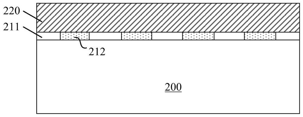
[0040] Please refer to figure 2 , providing a substrate 200, forming a first metal layer 212 and a dielectric layer 211 on the surface of the substrate 200; forming a magnetic tunnel junction structure layer 220 on the deposition surface of the first metal layer 212 and the dielectric layer 211.
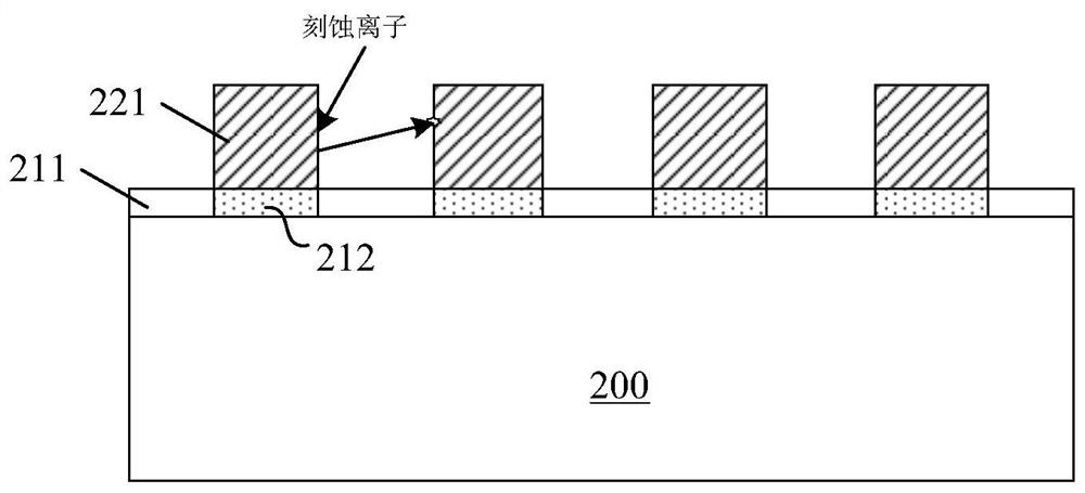
[0041] Please refer to image 3 , through the exposure and etching process, the magnetic tunnel junction structure layer 220 (please refer to figure 2 ) is patterned to form magnetic tunnel junction pillars 221 arranged in an array. Due to the higher requirements on the storag...
PUM
 Abstract
Description
Claims
Application Information