A composition for electron transport layer, electron transport layer and optoelectronic device

A technology of electron transport layer and optoelectronic device, which is applied in the direction of electric solid-state devices, electrical components, semiconductor devices, etc., can solve the problems of easy aging of electronic materials, interface damage, fast brightness decay, etc., and achieve the improvement of luminous efficiency and life. Effects of reducing injection barrier and driving voltage and improving short lifetime

Active Publication Date: 2022-07-19
JILIN OPTICAL & ELECTRONICS MATERIALS
View PDF7 Cites 0 Cited by
  • Summary
  • Abstract
  • Description
  • Claims
  • Application Information

AI Technical Summary

Problems solved by technology

With the development of OLED materials, organic materials that meet the performance requirements of OLED display panels tend to be electron-transporting. At room temperature, electron injection materials have no obvious impact on life, but at high temperatures, electron injection is slower than electron migration, resulting in electron transport. There is accumulation on the cathode side, and the electronic materials are easy to age, resulting in a shortened life of the OLED display panel
[0004] In addition, the light-emitting region of the device structure is close to the interface between the light-emitting layer and the hole, which is biased towards the electronic system. During the aging process of the life, the excitons have a greater impact on the interface on the HT side, resulting in damage to the interface, which affects the carrier injection. Affect the recombination of excitons, the efficiency is reduced, the brightness decays faster, and finally the life is poor
At present, an electron transport (ET) material and 8-hydroxyquinoline-lithium (Liq) doping technology are mostly used to solve the problem of electron injection and transport. The advantage of this structure is that the structure is relatively simple, but it has high requirements for ET materials and has high Electron mobility is conducive to improving device efficiency but leads to poor life. Although low electron mobility can guarantee life, it will lead to low device efficiency and rapid life decay at high temperatures.

Method used


Image

  • A composition for electron transport layer, electron transport layer and optoelectronic device
  • A composition for electron transport layer, electron transport layer and optoelectronic device
  • A composition for electron transport layer, electron transport layer and optoelectronic device

Examples


Embodiment 1

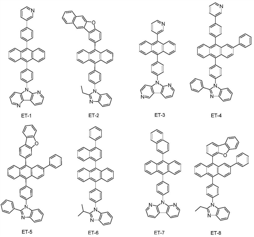
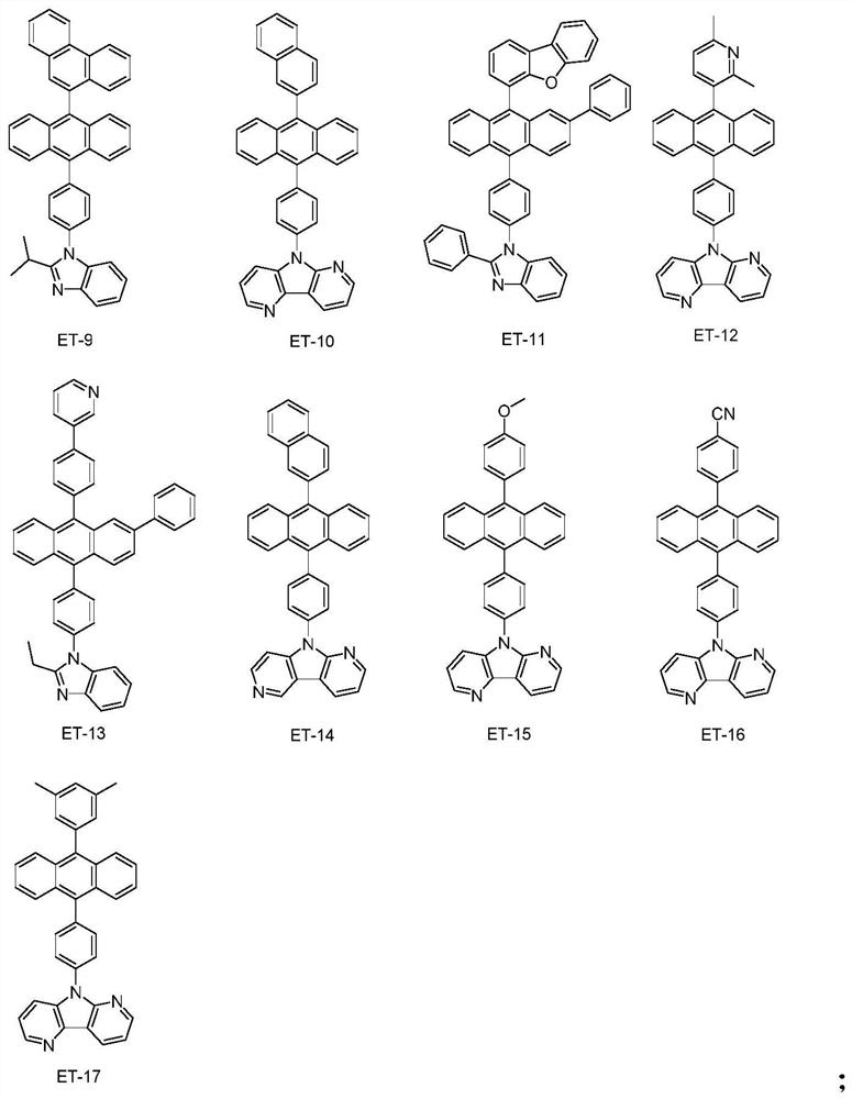
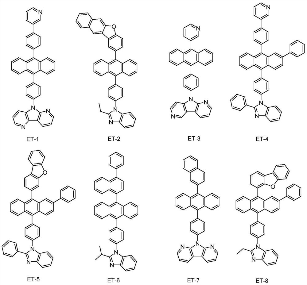
[0034] This example provides 17 kinds of electron transport materials, whose structural formulas are respectively formula ET-1 to formula ET-17, as shown below:

[0035]

[0036]

[0037] The electron mobility test is carried out on the electron transport materials whose structural formulas are respectively formula ET-1 to formula ET-17, and the test method is as follows:

[0038] Using vacuum evaporation equipment, vacuum evaporation is carried out on the substrate with ITO. Since the material to be tested is an electron transport material, a layer of electron blocking material with a thickness of 5nm is first evaporated. The test material and Liq, the thickness is 50nm, after the material to be tested is evaporated, the electron injection type material is evaporated, the thickness is 2nm, and finally a layer of cathode is evaporated, Ag can be used, and finally the SCLC space charge control current method is used to simulate Calculation, data collection of the material...

Embodiment 1

[0042] This embodiment provides an optoelectronic device, the preparation method of which includes the following steps:

[0043]S1. Clean the ITO / Ag / ITO film (ITO thickness is 14nm, Ag thickness is 150nm) on the glass substrate (150nm) of the OLED device in distilled water for 2 times, ultrasonically wash for 30 minutes, and repeatedly wash with distilled water for 2 times , ultrasonic cleaning for 10 minutes, after the distilled water cleaning is completed, isopropanol, acetone, methanol and other solvents are ultrasonically cleaned in sequence and then dried, transferred to the plasma cleaning machine, washed for 5 minutes, and sent to the evaporation machine.

[0044] S2. Compound N,N'-diphenyl-N,N'-bis(2-naphthyl)-1,1'-biphenyl-4,4'-diamine (NPB) with 2,3,5 , 6-tetrafluoro-7,7',8,8'-tetracyanoquinone-dimethane (F4-TCNQ) was introduced into the chamber of a vacuum vapor deposition apparatus at a doping ratio of 97:3, and the apparatus was then The pressure in the chamber i...

Embodiment 2

[0055] This embodiment provides an optoelectronic device, which is prepared according to the preparation method provided in the above device embodiment 1, the only difference is that the material ET-1 / ET-2 of the electron transport layer is replaced with the material in the material embodiment 1. ET-1 / ET-5.


PUM

PropertyMeasurementUnit
thicknessaaaaaaaaaa
thicknessaaaaaaaaaa
thicknessaaaaaaaaaa

Abstract

The invention discloses a composition for an electron transport layer, an electron transport layer and an optoelectronic device, belonging to the technical field of display. The composition comprises 8-hydroxyquinoline-lithium and a composite material; the composite material comprises at least two An electron transport material with a LUMO energy level of -2.95--2.70eV; the mass percentage content of 8-hydroxyquinoline-lithium in the composition is 40%-60%. The optoelectronic device containing the above composition enables faster electron injection and more balanced carrier recombination at high temperature, thereby improving the problem of short life at high temperature. In addition, by using electron transport materials with a reasonable energy level structure in the present invention, the energy levels in each layer of the optoelectronic device can form a stepped barrier, which can reduce the injection barrier and driving voltage. The carrier recombination is more balanced, which can effectively improve the luminous efficiency and lifetime of the device.

Description

technical field [0001] The present invention relates to the field of display technology, in particular to a composition for an electron transport layer, an electron transport layer and an optoelectronic device. Background technique [0002] Organic Light Emitting Diode (OLED) display panel is a self-luminous display panel. OLED display panel has the advantages of thinness, high brightness, low power consumption, wide viewing angle, high response speed and wide operating temperature range. It is more and more used in various high-performance display fields. Optoelectronic devices such as organic electroluminescent devices are generally multi-layered structures. Various auxiliary functional layers other than the light-emitting layer also play a crucial role in the performance of the device. A reasonable device structure can effectively improve the performance of the device. Electron injection Layers, electron transport layers, hole blocking layers, light emitting layers, elec...

Claims


Application Information

Patent Timeline
Patent Type & Authority Patents(China)
IPC IPC(8): H01L51/50H01L51/54
CPCH10K85/00H10K50/11H10K2101/40H10K50/16
Inventor 王铁邱镇姚明明王伟哲刘长伟杨勇马晓宇
Owner JILIN OPTICAL & ELECTRONICS MATERIALS
Why Eureka
Try Eureka