BMN multilayer dielectric film and preparation method thereof

A multilayer dielectric and thin film technology, applied in the field of microelectronics, can solve problems such as difficult control of dielectric film thickness and grain orientation

Active Publication Date: 2020-11-03
QILU UNIV OF TECH
View PDF11 Cites 2 Cited by
  • Summary
  • Abstract
  • Description
  • Claims
  • Application Information

AI Technical Summary

Problems solved by technology

This method has low preparation cost, simple operation, large film forming area, and is suitable for large-scale productio

Method used


Image

  • BMN multilayer dielectric film and preparation method thereof
  • BMN multilayer dielectric film and preparation method thereof
  • BMN multilayer dielectric film and preparation method thereof

Examples


preparation example Construction

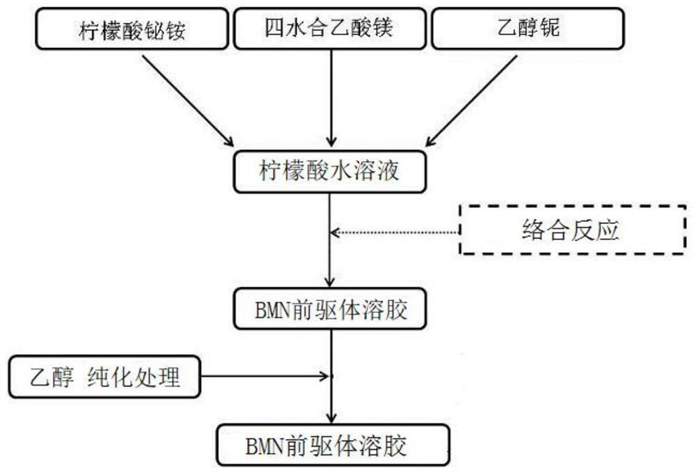
[0023] The invention provides a Bi 1.5 MgNb 1.5 o 7 A method for preparing a multilayer dielectric film, comprising the following steps:

[0024] Mix ammonium bismuth citrate, magnesium acetate tetrahydrate, niobium ethoxide and citric acid aqueous solution, and carry out complexation reaction to obtain Bi-Mg-Ni precursor sol;

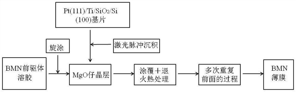
[0025] On Pt(111) / Ti / SiO by Laser Pulse Deposition 2 MgO is deposited on the surface of the / Si(100) substrate to obtain a MgO seed layer whose orientation is (111);

[0026] After coating the Bi-Mg-Ni precursor sol on the surface of the (111) MgO seed layer, performing annealing heat treatment to obtain a single-layer film;

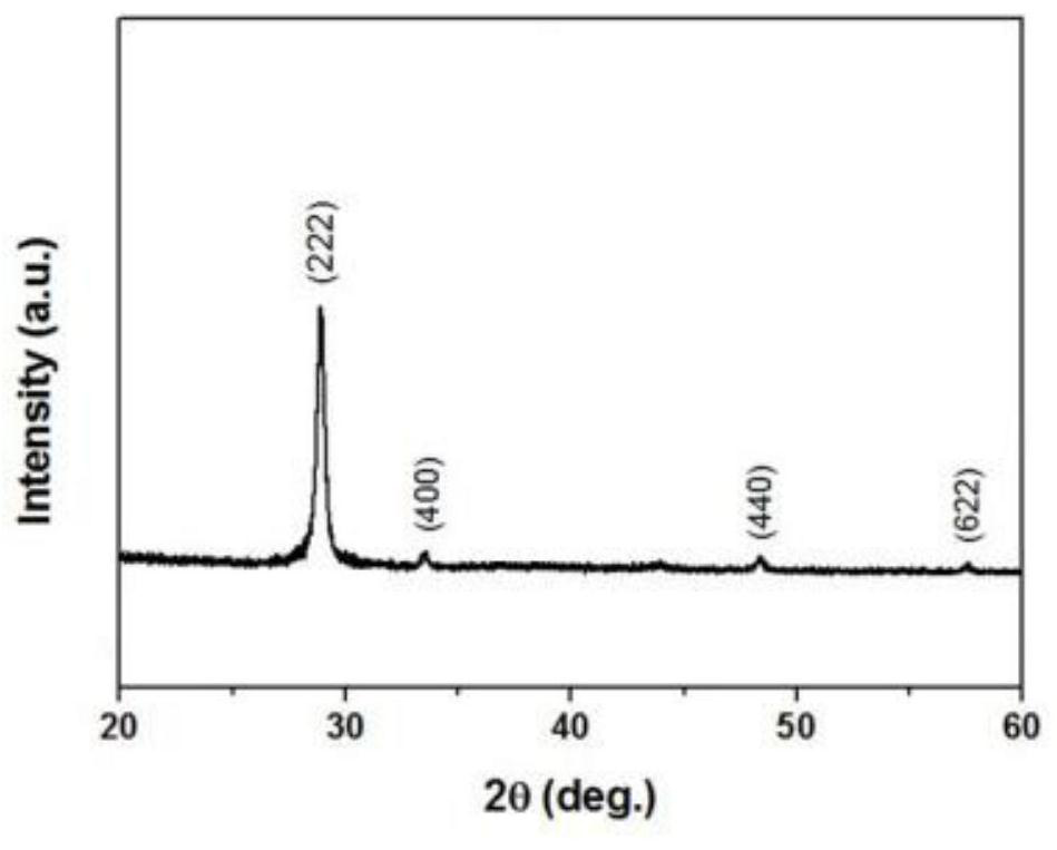
[0027] The single-layer film is repeatedly coated and annealed to obtain a BMN multilayer dielectric film with an orientation of (222).

[0028] In the present invention, unless otherwise specified, the raw materials used are conventional commercially available products in the field or prepared by conventional methods in the...

Embodiment 1

[0046] Pt(111) / Ti / SiO 2 / Si(100) substrates were ultrasonically cleaned in deionized water for 10 minutes, ultrasonically cleaned in acetone for 10 minutes, ultrasonically cleaned in ethanol for 10 minutes, and ultrasonically cleaned in deionized water for 10 minutes, and then dried under infrared lamps;

[0047] Press Bi 1.5 MgNb 1.5 o 7 The stoichiometric ratio of 5.8461g ammonium bismuth citrate, 1.3034g magnesium acetate tetrahydrate and 2.9008g niobium ethylate were added to 50mL citric acid aqueous solution (citric acid and deionized water were used as solvent, and its molar ratio was 1:10). Stir at 250°C to carry out the complexation reaction, and after 15 minutes, the complexation reaction product is obtained;

[0048] The complexation reaction product and ethanol were mixed in a volume ratio of 1:1, purified at room temperature and under ultrasonic conditions, and after 0.5h, a Bi-Mg-Ni precursor sol was obtained;

[0049] Under the conditions of oxygen pressure o...

Embodiment 2

[0055] Pt(111) / Ti / SiO 2 / Si(100) substrates were ultrasonically cleaned in deionized water for 10 minutes, ultrasonically cleaned in acetone for 10 minutes, ultrasonically cleaned in ethanol for 10 minutes, and ultrasonically cleaned in deionized water for 10 minutes, and then dried under infrared lamps;

[0056] Press Bi 1.5 MgNb 1.5 o 7 Weigh 11.6992g of ammonium bismuth citrate, 2.6068g of magnesium acetate tetrahydrate and 5.8016g of niobium ethoxide into 90mL of citric acid aqueous solution (the molar ratio of citric acid to deionized water is 1:20), at 500°C Under stirring, carry out complexation reaction, after 1h, obtain complexation reaction product;

[0057] Mix the complexation reaction product and ethanol at a volume ratio of 1:1.5, perform purification treatment at room temperature and ultrasonic conditions, and obtain a Bi-Mg-Ni precursor sol after 1 hour;

[0058] Under the condition that the oxygen pressure is 30Pa, the laser energy is 400mJ, the laser freq...


PUM

PropertyMeasurementUnit
Thicknessaaaaaaaaaa
Thicknessaaaaaaaaaa
The average particle sizeaaaaaaaaaa

Abstract

The invention provides a Bi1.5MgNb1.5O7 (BMN) multilayer dielectric film and a preparation method thereof, and belongs to the technical field of microelectronics. The preparation method provided by the invention comprises the following steps of mixing ammonium bismuth citrate, magnesium acetate tetrahydrate, niobium ethoxide and a citric acid aqueous solution, and carrying out a complexation reaction to obtain Bi-Mg-Ni precursor sol; carrying out deposition of MgO on the surface of a Pt (111)/Ti/SiO2/Si (100) substrate through a laser pulse deposition method, and obtaining an MgO seed crystallayer with the orientation being (111); coating the Bi-Mg-Ni precursor sol on the surface of the MgO seed crystal layer with the orientation being (111), and then carrying out annealing heat treatmentto obtain a single-layer film; repeating the coating and annealing heat treatment process on the single-layer film to obtain the BMN multilayer dielectric film with the orientation being (222).

Description

technical field [0001] The invention belongs to the technical field of microelectronics, and in particular relates to a BMN multilayer dielectric film and a preparation method thereof. Background technique [0002] With the increasing frequency of communication, wireless communication technology has entered the microwave field. Correspondingly, higher requirements are put forward for various communication equipment. Agile RF terminals must be designed and prepared to adapt to different microwave communication frequency bands. Tunable microwave devices that can be used in these communication devices, such as phase shifters, electronically adjustable filters, voltage-controlled oscillators, microwave switches, etc., are widely used in Microwave communication system has a wide range of applications. Varactors are the core of various adjustable microwave devices. The currently used adjustable microwave devices are mainly based on the following varactor technologies: semiconduct...

Claims


Application Information

Patent Timeline
IPC IPC(8): C23C18/12C23C14/28C23C14/08C23C28/04
CPCC23C18/1216C23C18/1254C23C18/1295C23C18/1225C23C14/28C23C14/081C23C28/04
Inventor 石锋
Owner QILU UNIV OF TECH
Why Eureka
Try Eureka