A kind of nanometer multi-layer coating and its preparation method and the cutter with nanometer multi-layer coating on the surface
A nano-multi-layer and nano-layer technology, which is applied in coating, metal material coating process, sputtering plating, etc., can solve the problems that hardness and thermal stability cannot be taken into account, and can not meet the requirements of high-speed cutting performance.
- Summary
- Abstract
- Description
- Claims
- Application Information
AI Technical Summary
Problems solved by technology
Method used
Image
Examples
preparation example Construction
[0027] The present invention provides the preparation method of the nano-multilayer coating described in the above technical solution, comprising the following steps:
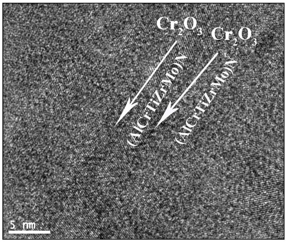
[0028] AlCrTiZrMo high-entropy alloy target and Cr alternately used in nitrogen and inert gas 2 O 3 Target, alternately cyclic magnetron sputtering deposition of (AlCrTiZrMo)N nanolayers and Cr on the substrate surface 2 O 3 nano-layers to obtain nano-multilayer coatings.
[0029]In the present invention, the substrate is preferably subjected to pretreatment before use, and the pretreatment preferably includes polishing, organic solvent washing, water washing, drying and vacuum ion cleaning performed in sequence. The present invention does not specifically limit the polishing method, and a polishing method well known to those skilled in the art may be used, such as mirror polishing. In the present invention, the organic solvent washing preferably includes anhydrous ethanol washing and acetone washing perfor...
Embodiment 1
[0043] (1) The substrate of the single crystal silicon wafer is subjected to mirror polishing treatment, and then ultrasonically cleaned with absolute ethanol, acetone and deionized water for 20 minutes under the condition of 30 kHz, and then dried, placed in a vacuum cleaning chamber, and evacuated to 6× 10 -4 After Pa, Ar was used as the ion source, and the vacuum degree was maintained at 4Pa. The high-speed steel substrate washed with deionized water was bombarded with intermediate frequency ions for 30min under the condition of 80W by radio frequency power supply, and the pretreated single crystal silicon wafer substrate was obtained.
[0044] (2) Place the pretreated single crystal silicon wafer substrate in a magnetron sputtering system, and alternately use AlCrTiZrMo high-entropy alloy targets with a purity of 99.99% and a diameter of 75 mm and Cr in nitrogen and an inert gas. 2 O 3 Target, alternately cyclic magnetron sputtering deposition of (AlCrTiZrMo)N nanolayers ...
Embodiment 2~5
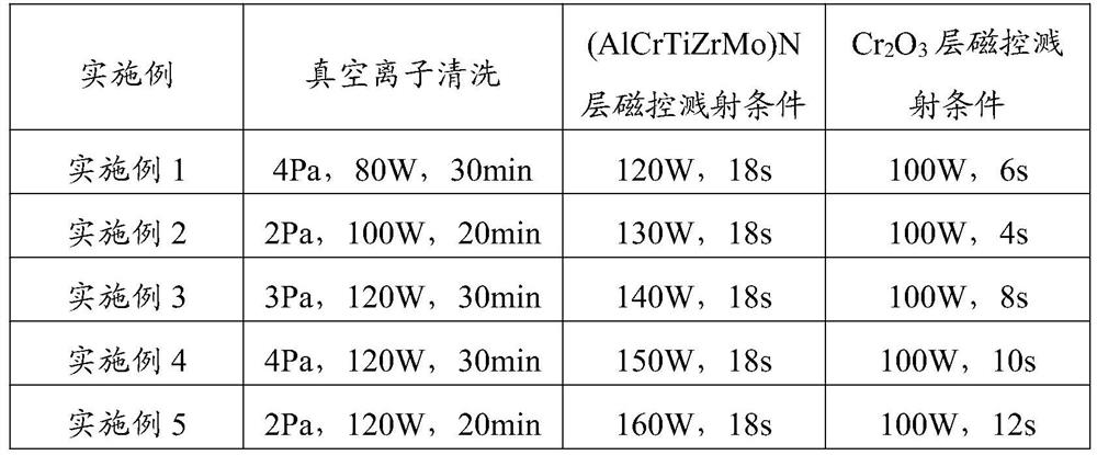
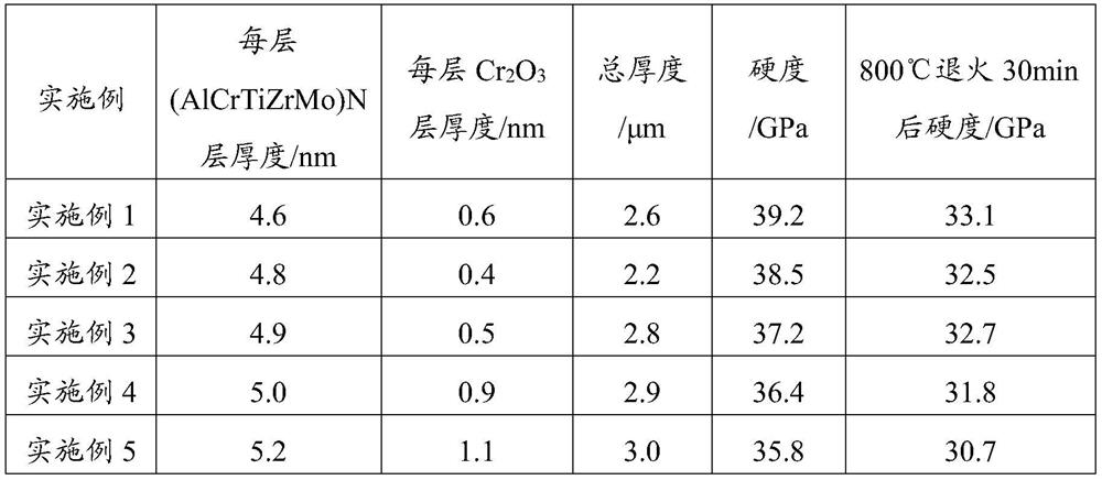
[0049] The nano-multilayer coating was prepared according to the method of Example 1, and the preparation conditions of Examples 1 to 5 are shown in Table 1:
[0050] Preparation conditions of Examples 1 to 5 in Table 1
[0051]
PUM
| Property | Measurement | Unit |
|---|---|---|
| thickness | aaaaa | aaaaa |
| thickness | aaaaa | aaaaa |
| thickness | aaaaa | aaaaa |
Abstract
Description
Claims
Application Information


