
Solar cell and manufacturing method thereof

A solar cell and manufacturing method technology, applied in circuits, photovoltaic power generation, electrical components, etc., can solve the problems of poor electrical conductivity, affecting the conversion efficiency of solar cells, large contact resistance, etc.

Active Publication Date: 2021-01-05
LONGI GREEN ENERGY TECH CO LTD
View PDF15 Cites 2 Cited by
  • Summary
  • Abstract
  • Description
  • Claims
  • Application Information

AI Technical Summary

Problems solved by technology

Due to the high work function of doped indium oxide, when doped indium oxide is in contact with the negative end of the cell, the contact resistance is large and the conductivity is poor, which affects the conversion efficiency of the solar cell.

Method used

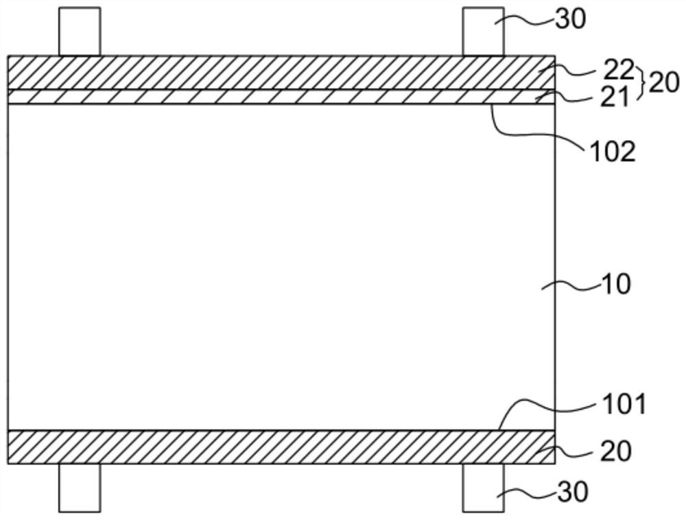
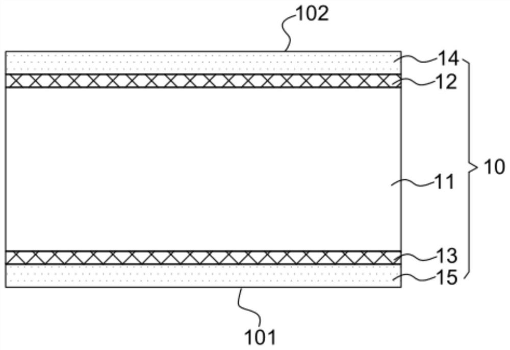
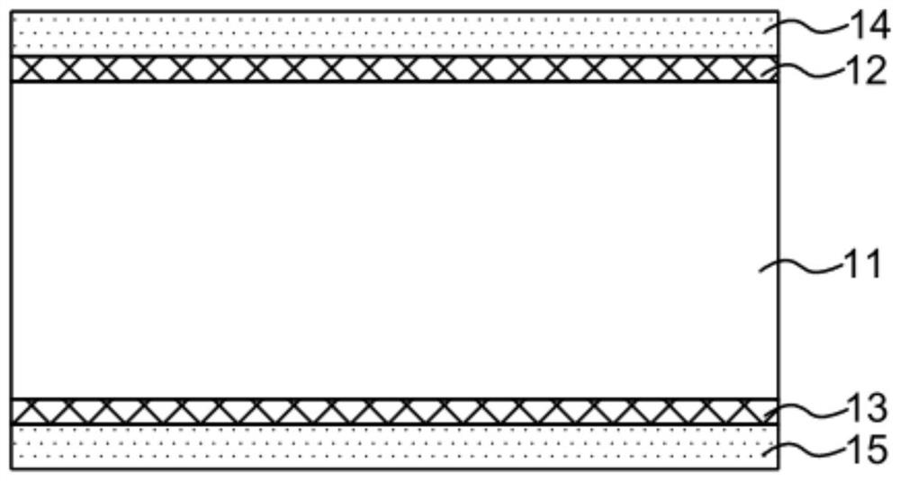

Image

  • Solar cell and manufacturing method thereof
  • Solar cell and manufacturing method thereof
  • Solar cell and manufacturing method thereof

Examples


Embodiment 1

[0075]The manufacturing method of the n-type silicon heterojunction solar cell provided in this embodiment is specifically as follows:

[0076]The first step is to provide an n-type crystalline silicon wafer. The n-type crystalline silicon wafer is sequentially polished, textured and cleaned to form an n-type crystalline silicon wafer with a textured surface.

[0077]In the second step, a PECVD process is used to deposit a first intrinsic amorphous silicon layer on the front side of the n-type crystalline silicon wafer, and a second intrinsic amorphous silicon layer on the back side of the n-type crystalline silicon wafer.

[0078]In the third step, a PECVD process is used to deposit an n-type doped amorphous silicon layer on the first intrinsic amorphous silicon layer.

[0079]In the fourth step, a PECVD process is used to deposit a p-type doped amorphous silicon layer on the second intrinsic amorphous silicon layer.

[0080]In the fifth step, a first transparent conductive film (with a thickness...

Embodiment 2

[0087]The manufacturing method of the n-type silicon heterojunction solar cell provided in this embodiment is specifically as follows:

[0088]The first step is to provide an n-type crystalline silicon wafer. The n-type crystalline silicon wafer is sequentially polished, textured and cleaned to form an n-type crystalline silicon wafer with a textured surface.

[0089]In the second step, a PECVD process is used to deposit a first intrinsic amorphous silicon layer on the front side of the n-type crystalline silicon wafer, and a second intrinsic amorphous silicon layer on the back side of the n-type crystalline silicon wafer.

[0090]In the third step, a PECVD process is used to deposit an n-type doped amorphous silicon layer on the first intrinsic amorphous silicon layer.

[0091]In the fourth step, a PECVD process is used to deposit a p-type doped amorphous silicon layer on the second intrinsic amorphous silicon layer.

[0092]In the fifth step, a first transparent conductive film (with a thickness...

Embodiment 3

[0099]The manufacturing method of the n-type silicon heterojunction solar cell provided in this embodiment is specifically as follows:

[0100]The first step is to provide an n-type crystalline silicon wafer. The n-type crystalline silicon wafer is sequentially polished, textured and cleaned to form an n-type crystalline silicon wafer with a textured surface.

[0101]In the second step, a PECVD process is used to deposit a first intrinsic amorphous silicon layer on the front side of the n-type crystalline silicon wafer, and a second intrinsic amorphous silicon layer on the back side of the n-type crystalline silicon wafer.

[0102]In the third step, a PECVD process is used to deposit an n-type doped amorphous silicon layer on the first intrinsic amorphous silicon layer.

[0103]In the fourth step, a PECVD process is used to deposit a p-type doped amorphous silicon layer on the second intrinsic amorphous silicon layer.

[0104]In the fifth step, a first transparent conductive film (with a thickness...


PUM

PropertyMeasurementUnit
thicknessaaaaaaaaaa
thicknessaaaaaaaaaa
electron work functionaaaaaaaaaa

Abstract

The invention discloses a solar cell and a manufacturing method thereof, relates to the technical field of photovoltaics, and aims to reduce the contact resistance between a transparent conductive layer and the negative electrode end of the solar cell and improve the conductivity. The solar cell comprises a cell piece with a positive electrode end and a negative electrode end, and a transparent conductive layer formed at the negative electrode end of the cell piece, wherein the transparent conductive layer comprises a first transparent conductive film and a second transparent conductive film;the first transparent conductive film and the second transparent conductive film are laminated along the direction far away from the negative electrode end of the battery piece; the first transparentconductive film contains ZnO doped with H atoms. The manufacturing method provided by the invention is used for manufacturing the solar cell.

Description

Technical field[0001]The invention relates to the field of photovoltaic technology, in particular to a solar cell and a manufacturing method thereof.Background technique[0002]Clean energy is one of the effective ways to solve the problems of energy shortage and environmental pollution, and photovoltaic power generation, as an important part of clean energy, has attracted much attention. In recent years, solar cell technology has developed rapidly.[0003]Most of the existing solar cells use doped indium oxide from the flat panel display (FDP) industry as the transparent conductive layer (TCO) material. Doped indium oxide is usually In2O3And SnO2Mixture, In2O3And SnO2The mass ratio is generally 90:10. Due to the high work function of doped indium oxide, when the doped indium oxide is in contact with the negative terminal of the cell, the contact resistance is large and the conductivity is poor, thereby affecting the conversion efficiency of the solar cell.Summary of the invention[0004]...

Claims


Application Information

Patent Timeline
Patent Type & Authority Applications(China)
IPC IPC(8): H01L31/075H01L31/0224H01L31/18C23C14/08C23C14/34C23C14/35C23C14/54C23C16/24C23C16/50C23C28/04
CPCH01L31/075H01L31/022425H01L31/022483H01L31/1884C23C14/3435C23C14/3457C23C14/54C23C14/086C23C14/35C23C16/24C23C16/50C23C28/04Y02E10/548Y02P70/50
Inventor 徐琛
Owner LONGI GREEN ENERGY TECH CO LTD
Learn More