

Micro-LED chip structure capable of reducing side wall defect recombination and preparation method
A chip structure and defect technology, applied in the direction of electrical components, circuits, semiconductor devices, etc., can solve the problem of Micro-LED luminous efficiency and uniformity, increase the conductivity of the middle position of the ITO layer, and prevent current from being bound in the middle of the device Area and other issues, to achieve the effects of reducing optical crosstalk effects, improving lateral confinement, and reducing non-radiative recombination effects
- Summary
- Abstract
- Description
- Claims
- Application Information
AI Technical Summary
Problems solved by technology
Method used
Image

Examples
preparation example Construction
[0045]The present invention is a method for preparing a novel Micro-LED chip structure with reduced sidewall defects. The steps of the method are as follows:
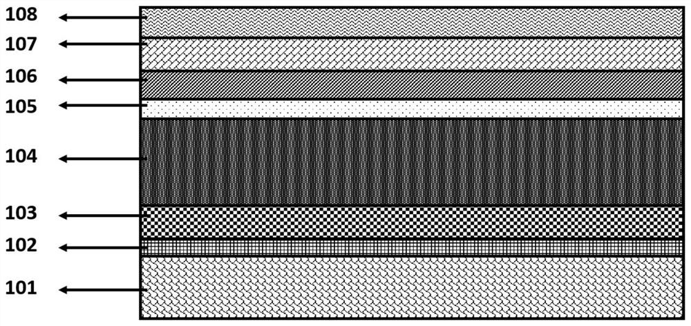
[0046]In the first step, the substrate 101 is cleaned with acetone, absolute ethanol, and deionized water in sequence in ultrasound, and the substrate 101 is cleaned by ultrasound for 5-10 minutes each time to remove foreign matter attached to the surface of the substrate 101;
[0047]In the second step, in the MOCVD or MBE reaction furnace, a buffer layer 102 with a thickness of 0.01 μm to 0.05 μm is epitaxially grown on the surface of the substrate 101 processed in the first step to realize the nucleation layer and release the lattice distortion. The stress caused by the distribution;
[0048]In the third step, in a MOCVD or MBE reaction furnace, a non-doped N-type semiconductor material layer 103 with a thickness of 2 μm-6 μm is epitaxially grown on the buffer layer 102 obtained in the second step at a high temperature to achieve t...
Embodiment 1
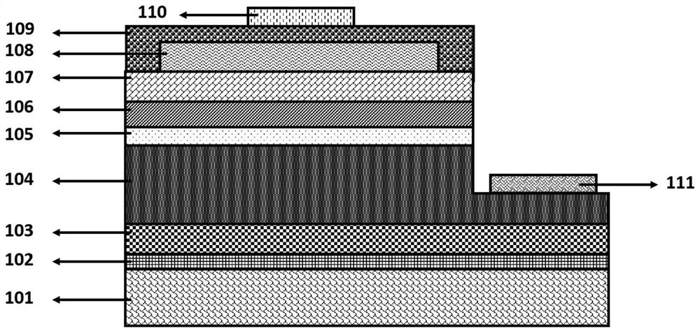
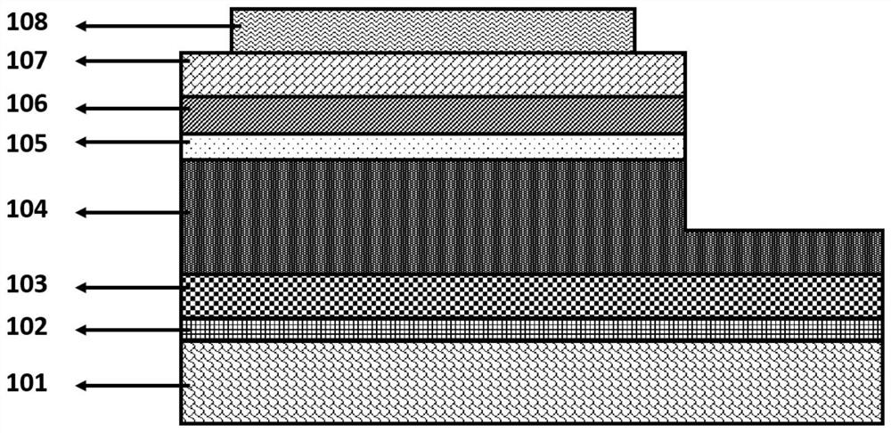
[0057]The present embodiment is a novel Micro-LED chip structure with reduced sidewall defect recombination. The epitaxial structure includes in order along the epitaxial growth direction: a substrate 101, a buffer layer 102, an undoped semiconductor material layer 103, and an N-type semiconductor material Layer 104, multiple quantum well layer 105, P-type confinement layer 106, P-type semiconductor material layer 107, P-type heavily doped semiconductor material layer 108, N-type material transport layer 109, P-type ohmic electrode 110, and N-type ohmic electrode 111 . Among them, the lateral size of the chip is 10 μm, the material of the N-type material transfer layer 109 is indium tin oxide, and the P-type heavily doped semiconductor material layer 108 is located in the middle area above the P-type semiconductor material layer 107, which occupies the P-type semiconductor material layer 107. 80% of the area, the N-type material transmission layer 109 directly contacts the P-type se...
Embodiment 2
[0076]The present embodiment is a novel Micro-LED chip structure with reduced sidewall defect recombination. The epitaxial structure includes in order along the epitaxial growth direction: a substrate 101, a buffer layer 102, an undoped semiconductor material layer 103, and an N-type semiconductor material Layer 104, multiple quantum well layer 105, P-type confinement layer 106, P-type semiconductor material layer 107, P-type heavily doped semiconductor material layer 108, N-type material transport layer 109, P-type ohmic electrode 110, and N-type ohmic electrode 111 . Among them, the lateral size of the chip is 30 μm, the material of the N-type material transport layer 109 is indium tin oxide, and the P-type heavily doped semiconductor material layer 108 is located in the middle area above the P-type semiconductor material layer 107, which occupies the P-type semiconductor material layer 107. 90% of the area, the N-type material transfer layer 109 directly contacts the P-type semic...
PUM
| Property | Measurement | Unit |
|---|---|---|
| Thickness | aaaaa | aaaaa |
| Thickness | aaaaa | aaaaa |
| Thickness | aaaaa | aaaaa |
Abstract
Description
Claims
Application Information