Supercharge Your Innovation With Domain-Expert AI Agents!

Preparation method of silicon-based OLED micro-display

A micro-display, silicon-based technology, applied in semiconductor/solid-state device manufacturing, semiconductor devices, electric solid-state devices, etc., can solve problems such as affecting electrode connectivity, corroding the metal in the electrode area, and poor electrode connection, so as to improve product yield , to ensure the effect of connectivity

Pending Publication Date: 2021-01-22
ANHUI SEMICON INTEGRATED DISPLAY TECH CO LTD
View PDF12 Cites 0 Cited by
  • Summary
  • Abstract
  • Description
  • Claims
  • Application Information

AI Technical Summary

Problems solved by technology

[0003] During the preparation of conventional silicon-based OLED microdisplays, when preparing the anode, anode insulating layer, OLED evaporation, cathode evaporation and thin film packaging, the electrodes on the CMOS circuit are exposed on the surface of the substrate. The anode, anode insulating layer, In the production of thin film encapsulation layer, flat layer and color film, alkaline agents such as developer are used many times. The alkaline agent may corrode the metal in the electrode area, resulting in too much thinning of the electrode metal, which affects the connection of the electrodes. Sex, resulting in poor electrode connection

Method used


Image

  • Preparation method of silicon-based OLED micro-display
  • Preparation method of silicon-based OLED micro-display
  • Preparation method of silicon-based OLED micro-display

Examples


Embodiment Construction

[0023] Specific embodiments of the present invention will be described in detail below in conjunction with the accompanying drawings. It should be understood that the specific embodiments described here are only used to illustrate and explain the present invention, and are not intended to limit the present invention.

[0024] In the present invention, unless stated otherwise, the orientation words included in the term such as "up, down, left, and right" only represent the orientation of the term in the normal use state, or the common name understood by those skilled in the art, rather than should be considered a limitation of the term.

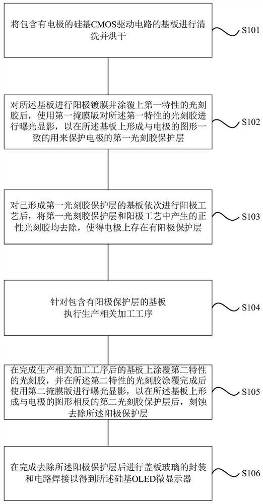
[0025] figure 1 It is a method for preparing a silicon-based OLED microdisplay of the present invention, such as figure 1 Shown, the preparation method of described silicon-based OLED microdisplay comprises:

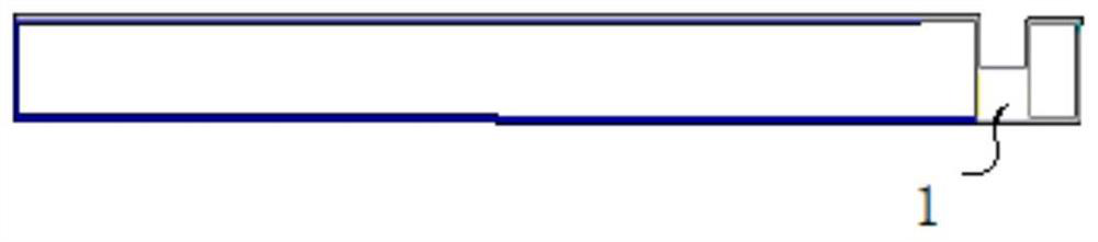
[0026] S101 , cleaning and drying the substrate of the silicon-based CMOS driving circuit including the electrode 1 . The substrate...


PUM


Abstract

The invention discloses a preparation method of a silicon-based OLED micro-display. The preparation method comprises the following steps: cleaning and drying a substrate of a silicon-based CMOS driving circuit containing an electrode; carrying out anodic coating on the substrate, coating photoresist with a first characteristic, and then carrying out exposure and development on the photoresist withthe first characteristic by using a first mask plate to form a first photoresist protection layer on the substrate; sequentially carrying out an anodic process on the substrate, and removing the first photoresist protection layer and positive photoresist generated in the anodic process, so an anodic protection layer exists on the electrode; performing a production-related processing step on the substrate including the anodic protection layer; coating the substrate with the photoresist with a second characteristic, carrying out exposure and development by using a second mask plate after the coating is finished, and performing etching to remove the anodic protection layer; after the anodic protection layer is removed, performing the packaging and circuit welding of the cover plate glass. According to the invention, the silicon-based OLED micro-display with no electrode corrosion phenomenon can be prepared.

Description

technical field [0001] The invention relates to the field of organic electroluminescent devices, in particular to a method for preparing a silicon-based OLED microdisplay. Background technique [0002] Silicon-based organic light-emitting diode (OLED, Organic Light Emitting Diode) microdisplay is a new type of display technology that manufactures active light-emitting devices OLED on silicon-based CMOS drive circuit substrates. It has been widely used in machine-worn helmets, gun sights , night vision devices and other military markets, and has extremely broad application prospects in the AR / VR market, and is known as the dark horse of the next generation of display technology. [0003] During the preparation of conventional silicon-based OLED microdisplays, when preparing the anode, anode insulating layer, OLED evaporation, cathode evaporation and thin film packaging, the electrodes on the CMOS circuit are exposed on the surface of the substrate. The anode, anode insulating...

Claims


Application Information

Patent Timeline
IPC IPC(8): H01L51/56H01L27/32
CPCH10K59/12H10K71/00
Inventor 孙云翔
Owner ANHUI SEMICON INTEGRATED DISPLAY TECH CO LTD
Features
  • R&D
  • Intellectual Property
  • Life Sciences
  • Materials
  • Tech Scout
  • Unparalleled Data Quality
  • Higher Quality Content
  • 60% Fewer Hallucinations
Learn More