Method for screening and matching insulating and heat-insulating material and nano-crystalline metal material in nano current channel layer

A technology of current channel and thermal insulation material, applied in the field of phase change storage, can solve the problems of high process process, high process cost and difficulty

Pending Publication Date: 2021-04-20
HUAZHONG UNIV OF SCI & TECH
View PDF0 Cites 1 Cited by
  • Summary
  • Abstract
  • Description
  • Claims
  • Application Information

AI Technical Summary

Problems solved by technology

Among them, the most direct way to change the device structure is to reduce the amount of phase-change materials while increasing the current density by reducing the size of the device, such as the restricted phase-change memory cell structure, etc., but this method requires a higher process and process cost high, difficult
Other methods to change the structure of the device, such as edge contact type, asymmetric structure, ring electrode structure, adding a two-dimensional material thermal resistance layer, etc., are all done by minimizing the phase transition without improving the process. The amount of material or the heat dissipation of the device can be reduced to reduce the write power consumption of the phase change unit, but these methods require major changes in the device structure and process, and there are problems of high process cost and difficulty

Method used


Image

  • Method for screening and matching insulating and heat-insulating material and nano-crystalline metal material in nano current channel layer
  • Method for screening and matching insulating and heat-insulating material and nano-crystalline metal material in nano current channel layer
  • Method for screening and matching insulating and heat-insulating material and nano-crystalline metal material in nano current channel layer

Examples


Embodiment 1

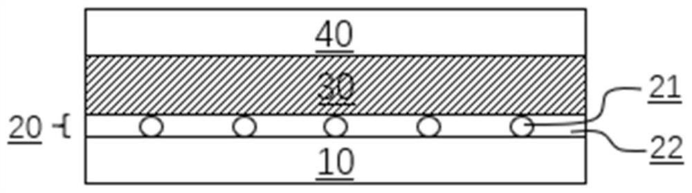
[0086] According to the first embodiment of the present invention, a cross-sectional view of an exemplary structure of a phase change memory having a nano-current channel layer to figure 2 Shows. Bottom electrode 10 is formed on SiO 2 On the substrate, the material of the bottom electrode 10 is selected from W, Pt, Au, Al, Cu, Ti, Ta and other metal materials and conductive materials of their alloys. The nano-current channel 20 is formed on the bottom electrode 10. The nano-current channel 20 is composed of insulating and heat-insulating material 22 and conductive nano-crystal grains 21 embedded in the middle of the insulating and heat-insulating material layer. The thickness of the nano-current channel layer 20 is 1 nm˜30 nm. The size of the conductive nanoparticles in the insulating layer is 1 nm˜30 nm, and the size of the conductive nanoparticles 21 in the direction perpendicular to the thin film is not less than the thickness of the nano current channel layer 20 . Compa...

Embodiment 2

[0089] According to the second embodiment of the present invention, finite element simulation is performed on the writing process of the phase-change memory structure with the nano-current channel layer and the conventional phase-change memory structure.

[0090] This simulation uses the simplest three-layer phase-change memory cell structure in Example 1. The material parameters used in the simulation are listed in Table 1 (the thermal and electrical parameters of the specific materials used in the finite element analysis). The upper and lower electrode materials of the two unit structures are Pt, and the insulating layer material is SiO 2 And the phase change layer material is Ge 2 Sb 2 Te 5 , the thickness of the upper and lower electrodes, the insulating layer, and the phase change layer are all 100 nm, and the diameter of the unit device is 100 nm. In the structure with the nano-current channel layer, the thickness of the nano-current channel layer is set to 5 nm, and t...

Embodiment 3

[0095] According to the third embodiment of the present invention, the manufacturing process of the T-type phase change memory cell containing the nano-current channel layer is as follows:

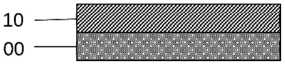
[0096] (1) Select SiO 2 / Si(100) substrate, the SiO 2 / Si(100) substrate was ultrasonicated with 40W power in acetone solution for 15 minutes to clean the surface, dust particles and organic impurities, and then rinsed with deionized water;

[0097] (2) Ultrasound the treated substrate with a power of 40w for 15 minutes in an ethanol solution, rinse with deionized water, and dry the surface and back of the substrate with high-purity N2 gas to obtain a substrate to be sputtered.

[0098] (3) As shown in FIG. 3(a), the bottom electrode 10 is grown on the substrate 00 using a magnetron sputtering method, and the bottom electrode 10 is made of Pt material, and high-purity argon gas is introduced as the sputtering gas during preparation, The sputtering gas pressure is 0.5 Pa, the power supply...


PUM

PropertyMeasurementUnit
thicknessaaaaaaaaaa
sizeaaaaaaaaaa
thicknessaaaaaaaaaa

Abstract

The invention discloses a method for screening and matching an insulating and heat-insulating material and a nano-crystalline metal material in a nano current channel layer. The method comprises the following steps: determining the insulating and heat-insulating material according to a material selection principle; establishing a crystal model according to the insulating material, heating the crystal model to melt the crystal model, cooling the crystal model to a preset first temperature, and operating the crystal model for a preset first time to obtain an amorphous model; calculating the formation energy, mean square displacement and radial distribution function of selected nano current channel material atoms in the model according to the amorphous model; and screening a material suitable for growing and gathering in the insulating and heat-insulating material according to the formation energy, the mean square displacement and the radial distribution function. The nano current channel layer prepared from the material screened by the method is an insulating layer containing metal nano crystal grains penetrating through the film thickness of the nano current channel layer, and the current only flows between the electrode layer and the phase change layer through a nano current channel formed by the metal nano crystal grains; and the power consumption of the phase-change memory can be obviously reduced.

Description

technical field [0001] The invention belongs to the technical field of phase change storage, and more particularly relates to a method for screening and matching an insulating and heat insulating material and a nanometer grain metal material in a nanometer current channel layer. Background technique [0002] With the advent of the information age, memory occupies an increasingly important position in life. At present, the research of memory has been developing in the direction of high speed, low power consumption and high stability. Among them, the phase-change memory (PCRAM) fabricated by utilizing the phase-change properties of materials has great potential in the semiconductor market. [0003] The basic principle of phase change memory is that phase change materials can be reversibly converted between crystalline and amorphous states, and use the huge difference in resistance between different states of the material to achieve "1" and "0" data storage. The commonly used ...

Claims


Application Information

Patent Timeline
Patent Type & Authority Applications(China)
IPC IPC(8): G16C60/00G16C10/00G06F30/20G06F111/08G06F119/08
Inventor 程晓敏李瀚曾运韬朱云来刘香君缪向水
Owner HUAZHONG UNIV OF SCI & TECH
Why Eureka
Try Eureka