
Two-dimensional material analog circuit, production method and application thereof

A technology of two-dimensional materials and analog circuits, which is applied in the manufacturing of circuits, electrical components, semiconductor/solid-state devices, etc., and can solve the problems of complex processes, complex circuits, and limited applications

Pending Publication Date: 2021-04-20
HUAZHONG UNIV OF SCI & TECH
View PDF3 Cites 0 Cited by
  • Summary
  • Abstract
  • Description
  • Claims
  • Application Information

AI Technical Summary

Problems solved by technology

[0004] The present invention provides a two-dimensional material analog circuit and its preparation method and application, which are used to solve the existing two-dimensional material p-n junction device and the circuit composed of it because of the use of a separate gate structure, which leads to complex circuits and complex processes and limited application. question

Method used


Image

  • Two-dimensional material analog circuit, production method and application thereof
  • Two-dimensional material analog circuit, production method and application thereof
  • Two-dimensional material analog circuit, production method and application thereof

Examples


Embodiment 1

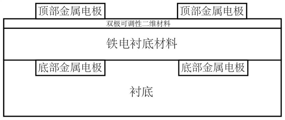
[0037] A two-dimensional material analog circuit, such as figure 1 As shown, including: substrate, bipolar tunable 2D material, thin film of ferroelectric substrate material, top metal electrode, and bottom metal electrode.

[0038] The bipolar tunable two-dimensional material and the ferroelectric substrate material film are stacked; the surface of the bipolar tunable two-dimensional material is provided with a top metal electrode; the surface of the ferroelectric substrate material film is provided with a bottom metal electrode; the ferroelectric The substrate material film is used to modulate the channel carrier type and concentration in the two-dimensional material under different polarization states; where the polarization of the ferroelectric substrate material film is passed between the top metal electrode and the bottom metal electrode Realized by external pulsed electric field.

[0039] According to the theory, the doping of two-dimensional materials can be induced b...

example 1

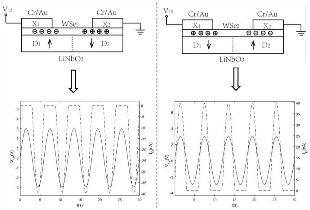
[0046] This example provides a ferroelectric substrate modulated rectifying p-n diode, its device structure and its test results are shown in figure 2 shown.

[0047] Among them, X 1 and x 2 is the top Cr / Au metal electrode, D 1 and D 2 Represents the two polarization states of the lithium niobate region. The upwardly polarized region will induce and accumulate electrons in the tungsten selenide channel, and the downwardly polarized region will induce and accumulate holes in the tungsten selenide channel, and the p-n junction of the two-dimensional material tungsten selenide is formed between the two . For the test results, the left figure shows the reverse connection of the p-n junction, and the input sinusoidal voltage V 12 (solid curve), the output current I D (Dashed curve indicates) only output reverse current, forward current is cut off; the right figure shows the forward connection of p-n junction, input sinusoidal voltage V 12 (solid curve), the output current...

example 2

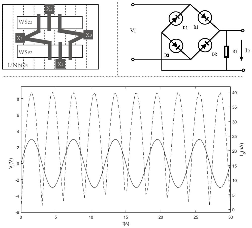
[0049] This example provides a ferroelectric substrate modulated bridge rectifier circuit, its device structure, equivalent circuit and its test results are as follows image 3 shown.

[0050] The device structure is presented by top view, in the figure X 1 -X 4 is the top Cr / Au metal electrode, and the bottom Au electrode is used to modulate the polarization state of lithium niobate (not shown in the figure), through periodic polarization modulation, so that X 1 with X 2 、X 3 with X 2 、X 4 with X 3 、X 4 with X 2 The p-n junctions are formed between the tungsten selenides below 1 、D 2 、D 3 、D 4 , at X 1 、X 3 Apply an input voltage V across the i , at X 2 、X 4 Both ends generate an output current I o , R 1 Load resistors are used to test current. The test result is that the sinusoidal voltage signal is input (indicated by the solid curve), and the output is a fully positive current signal (indicated by the dotted curve). Four diodes connected head to tail in...


PUM


Abstract

The invention belongs to the field of two-dimensional semiconductor circuits, and particularly relates to a two-dimensional material analog circuit, a production method and an application thereof. The two-dimensional material analog circuit comprises a substrate, a bipolar adjustable two-dimensional material, a ferroelectric substrate material film, a top metal electrode and a bottom metal electrode, wherein the two-dimensional material and the ferroelectric substrate material film are laminated; the top metal electrode is arranged on the surface of the two-dimensional material; the bottom metal electrode is arranged on the surface of the ferroelectric substrate material film; the ferroelectric substrate material film is used for modulating the type and concentration of channel carriers in the two-dimensional material in different polarization states; and polarization of the ferroelectric substrate material film is achieved by externally connecting a pulsed electric field between the top metal electrode and the bottom metal electrode. According to the invention, the electric field is removed after the ferroelectric substrate material is polarized, and only the polarization state of the ferroelectric substrate material is utilized to regulate and control the channel carriers of the two-dimensional material so that the power consumption is greatly reduced; and meanwhile, the two-dimensional material channel is regulated and controlled by setting different polarization states of the ferroelectric, and a reconfigurable circuit storage and calculation capacity is achieved.

Description

technical field [0001] The invention belongs to the field of two-dimensional semiconductor circuits, and more specifically relates to a two-dimensional material analog circuit and its preparation method and application. Background technique [0002] Traditional analog circuits are mainly based on silicon-based transistor devices, which have good performance in terms of threshold voltage, switching ratio, and gain. However, as the device size is further reduced, the short-channel effect of traditional silicon-based semiconductor devices will greatly reduce the performance of the device. Decline, Moore's Law reached the bottleneck. Finding new material systems and corresponding device structures to overcome the above bottlenecks is the current research direction. In the new material system, two-dimensional materials with atomic layer thickness have a variety of unique and excellent properties, including compatibility with existing semiconductor processes, miniaturization, hig...

Claims


Application Information

Patent Timeline
IPC IPC(8): H01L29/778H01L29/06H01L21/335H01L29/18H01L29/12
Inventor 叶镭彭追日童磊李政缪向水
Owner HUAZHONG UNIV OF SCI & TECH
Learn More