
Growth method of gallium-doped Czochralski single crystal silicon, gallium-doped single crystal silicon and its application

A growth method and monocrystalline silicon technology, which is applied in the growth of gallium-doped Czochralski monocrystalline silicon, gallium-doped monocrystalline silicon and its applications, can solve the problem of wide distribution range of resistivity of gallium-doped monocrystalline silicon, high cost of use, and battery problems. problems such as reduction

Active Publication Date: 2021-12-07
杭州晶宝新能源科技有限公司
View PDF0 Cites 0 Cited by
  • Summary
  • Abstract
  • Description
  • Claims
  • Application Information

AI Technical Summary

Problems solved by technology

[0003] However, because the segregation coefficient of gallium in silicon is 0.008, the too small segregation coefficient leads to a wide range of resistivity distribution of gallium-doped single crystal silicon, thus reducing the proportion of suitable cells in the crystal
If this technical problem is not solved, the cost of using gallium-doped single crystal silicon will be significantly higher than that of boron-doped single crystal silicon, which is not conducive to its industrial application

Method used


Image

  • Growth method of gallium-doped Czochralski single crystal silicon, gallium-doped single crystal silicon and its application
  • Growth method of gallium-doped Czochralski single crystal silicon, gallium-doped single crystal silicon and its application
  • Growth method of gallium-doped Czochralski single crystal silicon, gallium-doped single crystal silicon and its application

Examples


Embodiment 1

[0050] This embodiment provides a method for growing gallium-doped Czochralski single crystal silicon, which specifically includes the following steps:

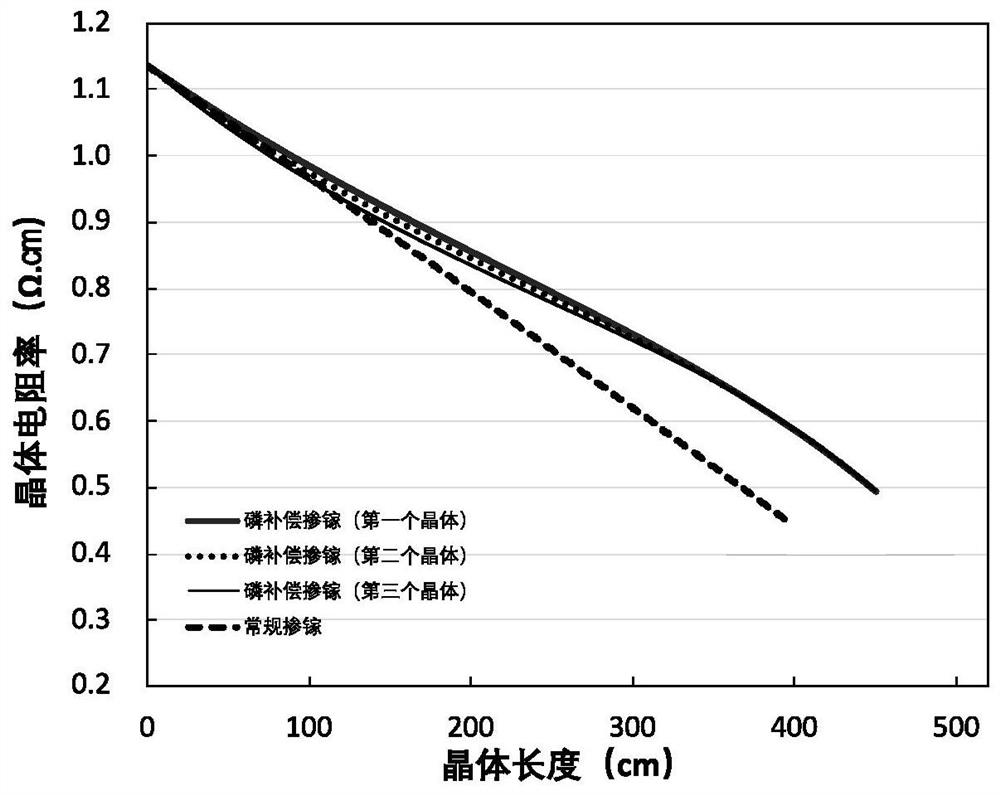
[0051] 580 kg of high-purity polysilicon raw material was charged into a crucible, and 48 g of high-purity gallium metal was added. The crucible is loaded into a crystal growth furnace, heated and melted to form a silicon melt, and gallium-doped Czochralski single crystal growth is carried out according to the Chester Czochralski single crystal method. Complete the necking and shouldering, enter the equal-diameter growth stage, set the diameter to 228mm, and the crystal grows stably at a rate of 2mm / min, then the crystal growth rate v is 81.7cm 3 / min. The gaseous donor dopant is configured, and the high-purity phosphine gas is diluted 100 times with high-purity argon gas, that is, the concentration is 1% by volume. Set the initial doping rate V D (1) is 2.4×10 -6 mol / min, converted into an effective donor gas flow rate o...

Embodiment 2

[0054] This embodiment provides a method for growing gallium-doped Czochralski single crystal silicon. The same parameters as in embodiment 1 are used to grow gallium-doped single crystal silicon crystals. The main difference lies in the adjustment of the use of gaseous donor dopants, as follows:

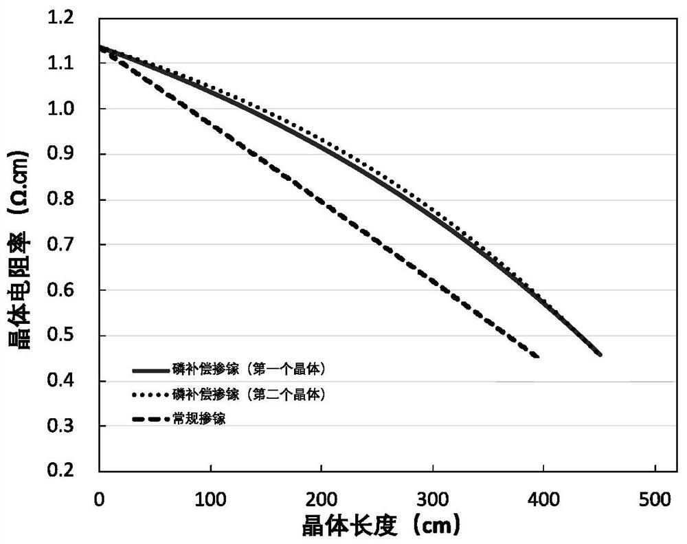
[0055] Set the doping rate V D (1)=2.0×10 -6 mol / min, the converted effective flow rate is 4.4mL / min. Use a program to control the flow, so that the flow changes uniformly with time. Set the time function q(t)=t / 300min, t(min), and feed the gaseous donor dopant according to the operating flow rate Q(t)=t / 300*4.4mL / min. When the crystal grows to a length of about 4.5 meters and the solidification ratio g is 0.75, stop feeding the donor gas, and then start to enter the finishing and follow-up procedures.

[0056] The test shows that the resistivity of the head is about 1.1Ω.㎝, and that of the tail is about 0.5Ω.㎝. Refill the high-purity polysilicon raw material according to the ab...


PUM


Abstract

The invention discloses a growth method of gallium-doped Czochralski single crystal silicon, gallium-doped single crystal silicon and its application, and relates to the technical field of single crystal silicon. In this growth method, polysilicon raw materials and gallium dopants are heated to the silicon melt, and silicon crystals are grown by Chester Czochralski single crystal method, and gaseous phosphorus dopants or arsenic dopants are introduced during the growth stage of silicon crystals. as a donor dopant. The inventor creatively introduces a gaseous donor dopant, which can significantly increase the solidification ratio, and can grow larger-quality silicon crystals in the same quality silicon melt, thereby significantly improving the crystal production efficiency. The gallium-doped single crystal silicon prepared by the above method has a narrower resistivity distribution and low preparation cost, and can be applied in solar cells.

Description

technical field [0001] The invention relates to the technical field of single crystal silicon, and in particular to a growth method of gallium-doped Czochralski single crystal silicon, gallium-doped single crystal silicon and its application. Background technique [0002] Solar cells based on the semiconductor photovoltaic effect have been widely used. The current mainstream solar cells are based on silicon crystal materials, especially single crystal silicon crystal materials, and silicon crystals must be doped to serve as the matrix material of solar cells. Among them, boron doping is more commonly used, and the segregation coefficient of boron in silicon is 0.8, which makes it easy to grow silicon crystals with uniform distribution of axial resistivity, which is suitable for the application of solar cells. However, due to the interaction between boron and oxygen, another unavoidable impurity in single crystal silicon, there is a phenomenon of efficiency attenuation in the...

Claims


Application Information

Patent Timeline
Patent Type & Authority Patents(China)
IPC IPC(8): C30B15/04C30B29/06H01L31/0288H01L31/18
CPCC30B15/04C30B29/06H01L31/0288H01L31/18Y02E10/50Y02P70/50
Inventor 陈鹏李晓强
Owner 杭州晶宝新能源科技有限公司
Learn More