A full-spectrum perovskite nanowire array and its preparation method

A nanowire array and perovskite technology, applied in nanotechnology, nanotechnology, chemical instruments and methods, etc., can solve the problems of inability to prepare and cumbersome operation process, and achieve the effect of easy physical properties, convenient operation and complete structure

Active Publication Date: 2022-04-01
JIHUA LAB
View PDF0 Cites 0 Cited by
  • Summary
  • Abstract
  • Description
  • Claims
  • Application Information

AI Technical Summary

Problems solved by technology

[0004] However, in the prior art, the use of single crystal nanowires for ion exchange to obtain full-spectrum perovskite nanowires requires the assistance of electron beam lithography methods, and needs to be carried out under a microscopic system. The operation process is cumbersome and impossible. Prepared from a macro perspective

Method used


Image

  • A full-spectrum perovskite nanowire array and its preparation method
  • A full-spectrum perovskite nanowire array and its preparation method
  • A full-spectrum perovskite nanowire array and its preparation method

Examples


preparation example Construction

[0049] Specifically, a method for preparing a full-spectrum perovskite nanowire array includes the following steps:

[0050] S1. Prepare the perovskite precursor solution in which the halogen group is bromine, that is, prepare the solute with the general molecular formula ABX 3 In X is the solution of the perovskite of Br;

[0051] S2, using a perovskite precursor solution to prepare a perovskite nanowire array;

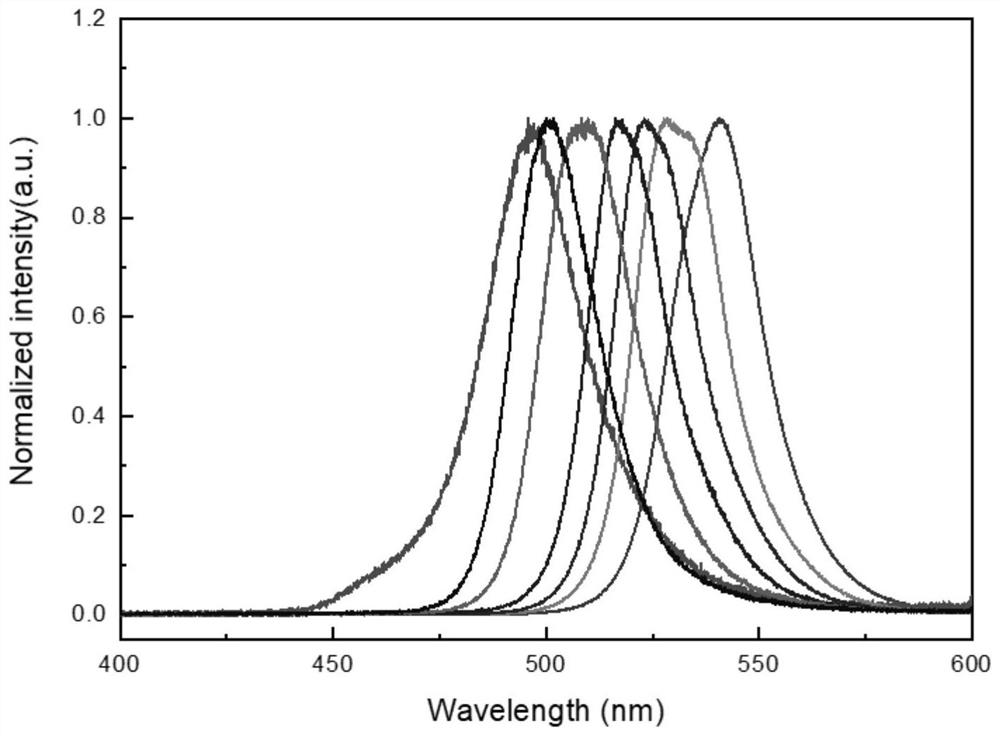
[0052] S3, prepare two kinds of ion exchange solutions containing chlorine and iodine in the solute respectively, for reaction replacement of bromine groups in the perovskite nanowire array;

[0053] S4. Soak one end of the perovskite nanowire array in an ion exchange solution thereof, and continuously pull the perovskite nanowire array; specifically, the perovskite nanowire array is fixed on the pulling rod of the pulling instrument through a clamp , and put the corresponding ion exchange solution in the crucible of the pulling instrument. During the ion exchange ...

Embodiment 1

[0090] S1, methylamine bromide (MABr) and lead bromide (PbBr 2 ) is dissolved in a mixed solution of N,N-dimethylformamide (DMF) and dimethyl sulfoxide (DMSO) with a volume ratio of 1:1 at a molar mass ratio of 1:1, and is configured as a precursor with a concentration of 20 mg / ml Bulk solution, that is, MAPbBr formulated with bromine as the halogen group 3 Perovskite precursor solution;

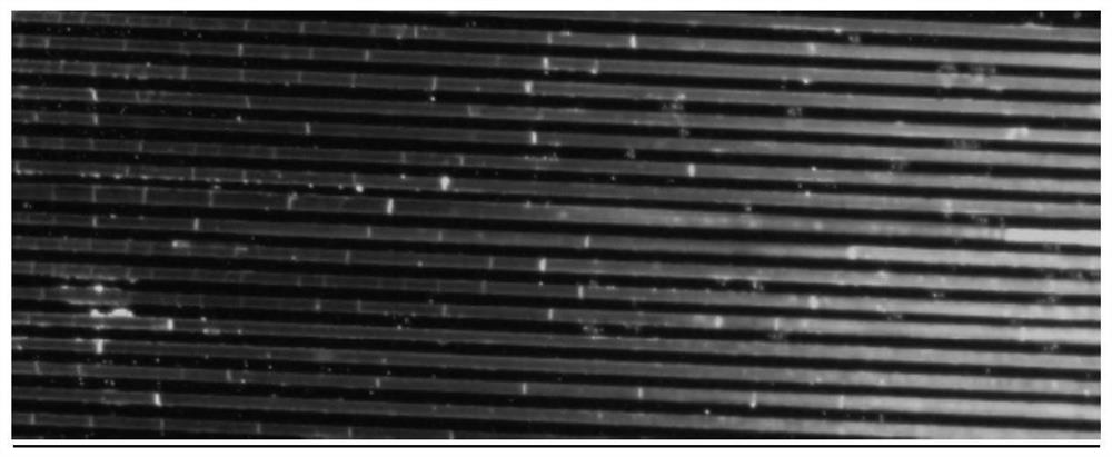
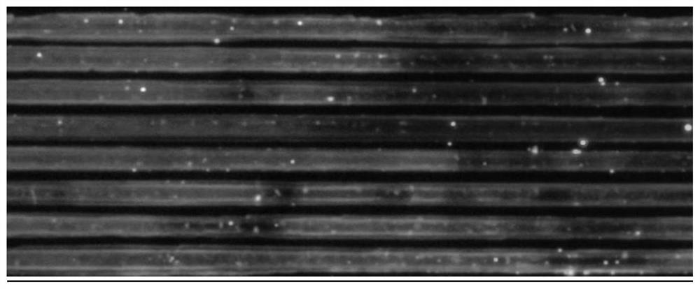
[0091] S2. Take 20 μL of MAPbBr 3 The perovskite precursor solution is directly added dropwise on the silica substrate, and the silicon pillar template containing the silicon pillar array is covered on the substrate to form a sandwich assembly system of substrate-perovskite precursor solution-silicon pillar template, and Place it in a vacuum oven at 60°C and heat it for 12 hours to crystallize by using the dewetting behavior. After the cooling sandwich assembly system is disassembled, MAPbBr can be obtained 3 Nano single crystal array;

[0092] S3, prepare two kinds of ion-exchange solut...

Embodiment 2

[0106] S1, cesium bromide (CsBr) and lead bromide (PbBr 2 ) is dissolved in a mixed solution of N,N-dimethylformamide (DMF) and dimethyl sulfoxide (DMSO) with a volume ratio of 1:1 at a molar mass ratio of 1:1, and is configured as a precursor with a concentration of 20 mg / ml Bulk solution, that is, the preparation of CsPbBr whose halogen group is bromine 3 Perovskite precursor solution;

[0107] S2. Take 20 μL of CsPbBr 3 The perovskite precursor solution is directly added dropwise on the silica substrate, and the silicon pillar template containing the silicon pillar array is covered on the substrate to form a sandwich assembly system of substrate-perovskite precursor solution-silicon pillar template, and Place in a vacuum oven at a temperature of 60°C and heat for 12 hours, crystallize by using the dewetting behavior, and CsPbBr can be obtained after cooling the sandwich assembly system and disassembling it. 3 Nano single crystal array;

[0108] S3, prepare two kinds of ...


PUM


Abstract

The invention discloses a full-spectrum perovskite nanowire array and a preparation method thereof. The preparation method of the full-spectrum perovskite nanowire array includes the following steps: preparing a perovskite precursor solution in which the halogen group is bromine; using Prepare the perovskite nanowire array from the perovskite precursor solution; prepare two ion exchange solutions containing chlorine and iodine in the solute; soak one end of the perovskite nanowire array in one of the ion exchange solutions, and continue to raise the Pull the perovskite nanowire array; take out the perovskite nanowire array that forms a heterojunction at one end, wash and dry; soak the other end of the perovskite nanowire array in another ion exchange solution, and continue to lift Pulling the perovskite nanowire array; taking out the perovskite nanowire array that also forms a heterojunction at the other end, cleaning and drying. The preparation method can directly and conveniently manufacture a characteristic spectrum perovskite nanowire array with a full-band spectrum directly from a macroscopic perspective.

Description

technical field [0001] The invention relates to the technical field of photoelectric materials, and mainly relates to a full-spectrum perovskite nanowire array and a preparation method thereof. Background technique [0002] Perovskite refers to a synthetic material with the same crystal form as calcium titanate, and its general molecular formula is ABX 3 , where the A and B sites are cations of different sizes, and X is a halide anion (X=Cl, Br, I); organic-inorganic hybrid perovskite materials have excellent photoelectric properties due to their diverse components and dimensions And photovoltaic characteristics, widely used in optoelectronic devices such as solar cells, light-emitting diodes, photodetectors, and nano-lasers. In the perovskite material system, nanocrystals can undergo rapid anion exchange reactions in solid-liquid or solid-gas states, and can control their composition ratio and electrical and optical properties. Therefore, ion exchange methods can be used t...

Claims


Application Information

Patent Timeline
Patent Type & Authority Patents(China)
IPC IPC(8): C30B7/14C30B29/12C30B29/60B82Y30/00B82Y40/00
CPCC30B7/14C30B29/12C30B29/60B82Y30/00B82Y40/00
Inventor 付悦吴雨辰江雷
Owner JIHUA LAB
Why Eureka
Try Eureka