Method and device for improving surface mobility of silicon carbide lateral double-diffusion field effect transistor

A lateral double diffusion, field effect transistor technology, applied in the field of wide bandgap power semiconductor devices, can solve the problems of reduced carrier mobility, high on-resistance, poor forward conduction characteristics, etc.

Active Publication Date: 2021-06-11
SOUTHEAST UNIV
View PDF6 Cites 2 Cited by
  • Summary
  • Abstract
  • Description
  • Claims
  • Application Information

AI Technical Summary

Problems solved by technology

However, since the current path of SiC LDMOS is under the oxide layer, the surface traps in the oxide layer will reduce the mobility of carriers and affect the transport of carriers. Therefore, the conventional SiC LDMOS has a high on-resistance, positive Poor conduction characteristics

Method used


Image

  • Method and device for improving surface mobility of silicon carbide lateral double-diffusion field effect transistor
  • Method and device for improving surface mobility of silicon carbide lateral double-diffusion field effect transistor
  • Method and device for improving surface mobility of silicon carbide lateral double-diffusion field effect transistor

Examples


Embodiment 1

[0022] A method for improving the surface mobility of silicon carbide lateral double-diffused field effect transistors. The method introduces a voltage bias tube. When the silicon carbide LDMOS transistor is forward-conducting, the high voltage in the drift region of the voltage bias tube can be transmitted to the Multiple polysilicon field plates above the surface of the drift region of the SiC LDMOS transistor. The high voltage on the polysilicon field plate has the effect of attracting electrons, which makes the surface of the drift region of the LDMOS tube gather electrons, increase the electron concentration, reduce the probability of a single electron being captured by the traps on the surface of the oxide layer above the drift region, and increase the electron mobility.

Embodiment 2

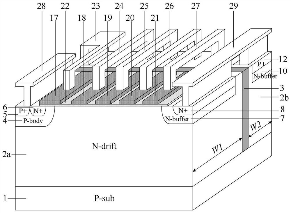
[0024] In general, the silicon carbide lateral double-diffused metal oxide semiconductor field effect transistor with high surface mobility of the present invention is composed of LDMOS with multiple polysilicon field plates and a voltage bias transistor.

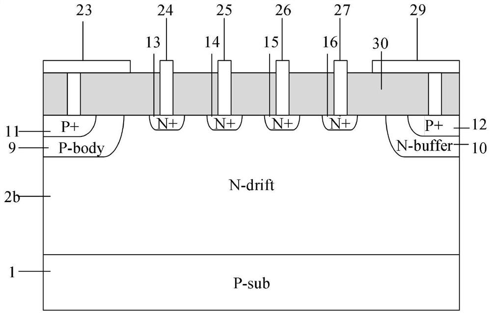
[0025] Combine below figure 2 image 3 , the present invention is described in detail:

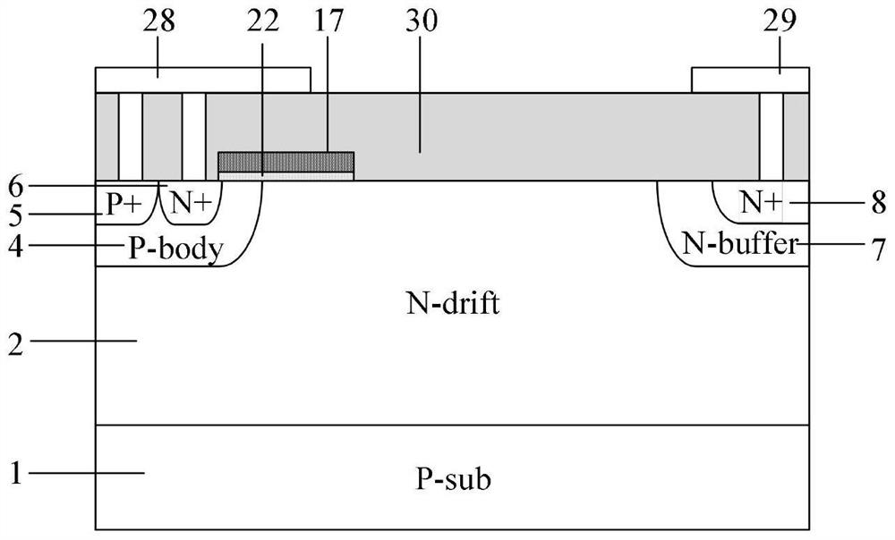
[0026]A device used in the method for improving the surface mobility of silicon carbide lateral double-diffused field effect transistors, comprising: a P-type substrate 1, an N-type drift region 2 is arranged on the P-type substrate 1, and an N-type drift region 2 is arranged on the N-type drift region. A P-type isolation layer 3 is provided in the region 2 and is divided into a first N-type drift region 2a and a second N-type drift region 2b by the P-type isolation layer 3, and a second N-type drift region 2a is respectively provided on the first N-type drift region 2a. A P-type base region 4 and the first N-type buffer layer 7 are ...


PUM

PropertyMeasurementUnit
widthaaaaaaaaaa
lengthaaaaaaaaaa
widthaaaaaaaaaa

Abstract

The invention discloses a method and device for improving the surface mobility of a silicon carbide lateral double-diffusion field effect transistor. The method comprises the steps: introducing a voltage bias tube, enabling the surface electron concentration of a drift region to be increased when a silicon carbide LDMOS is in forward conduction, enabling the probability that a single electron is captured by a surface trap of an oxide layer above the drift region to be reduced, and enabling the electron mobility to be improved. The device comprises a P-type substrate, which is provided with a P-type isolation layer which divides the device into an LDMOS and a voltage bias tube, the LDMOS comprises a first N-type drift region, a first source region, a first drain region, a gate oxide layer and a polysilicon gate, and is characterized in that four polysilicon field plates which are separated from one another are arranged on the gate oxide layer, the voltage bias tube comprises a second N-type drift region, a second source region and a second drain region, four N+ injection layers are arranged in the second N-type drift region, the polysilicon gate is connected with the second source region, the first drain region is connected with the second drain region, and the four polysilicon field plates are respectively connected with the four N+ injection layers.

Description

technical field [0001] The present invention mainly relates to the technical field of wide-bandgap power semiconductor devices, in particular to a method and device for improving the surface mobility of silicon carbide lateral double-diffusion field effect transistors, which are suitable for many power control and processing fields such as switching power supplies and inverters. In order to reduce the on-state loss of the device in the case of forward conduction. Background technique [0002] Double-diffused MOSFET (DMOS) has the characteristics of high current, high voltage resistance, and high switching speed. It is widely used in the fields of switching power supply, household appliances, smart grid and traffic transmission. There are two main types of DMOS, VDMOSFET (VerticalDouble-diffused MOSFET) and LDMOSFET (LateralDouble-diffused MOSFET), among which LDMOS is easier to compare with CMOS Process compatible applications are more extensive. [0003] In recent years,...

Claims


Application Information

Patent Timeline
Patent Type & Authority Applications(China)
IPC IPC(8): H01L29/78H01L29/40
CPCH01L29/7816H01L29/7818H01L29/404
Inventor 张龙崔汪明马杰祝靖孙伟锋时龙兴
Owner SOUTHEAST UNIV
Why Eureka
Try Eureka